netZener.net
-
Home

- Project Articles
Portable Variable Power Supply - Part 2
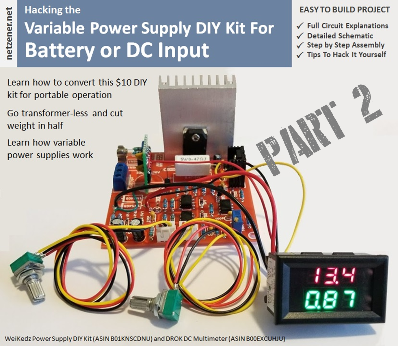
This is the second installment of the Portable Variable Power Supply article. In Part 1, I described in detail each building block of the Weikedz power supply kit and highlighted the strengths and weaknesses of the design. Now in Part 2, I'll show you how to use all of the information gained to adapt the Weikedz power supply for portable applications.
Batteries for portable devices

My initial concern with this project was finding a reliable supplier of rechargeable cells that were small, light, easy to use, and cost effective. Turns out a totally different problem would lead me to the exact product and company I needed:
While I was working on this project, one of the battery packs failed on my DeWalt 12V drill/screwdriver. The thing cost me $90 bucks at Home Depot about 18 months ago so I was hoping to find a replacement pack for maybe $20 to $30. Ha. No such luck. The best I could do was $60 for a single pack from DeWalt.
For that price I might as well buy another screw driver. But then I thought, "There has to be a way I can avoid playing the manufacturers planned obsolescence game." So I ignored the dire warnings in bold large print on the manual and disassembled the failed battery pack. Wouldn't you know it was stuffed with three 18650 cells in series and a little charge control circuit board. Checking voltages on each revealed one cell with zero volts; open circuit.
A quick google search and I had thousands of hits. But one vendor popped to the top with exactly the cell I needed: liionwholesale.com
They had the exact part number I needed for just a few bucks. They processed my order on a Sunday (no kidding... Sunday), and shipped first thing Monday morning. The cell was a perfect fit and immediately restored my battery pack to operation. Now I don't have to avoid rechargeable tools because the manufacturers want exorbitant prices for a battery pack. The batteries used for the Portable Variable Power Supply project were ordered from liionwholesale.com. Give them a try because they have a huge selection of protected, unprotected, low ESR, and high capacity cells. And some really good prices as well.
A quick re-summary
The point of the previous article was to deconstruct the WeiKedz Variable Power supply and examine each function block and component to describe what they do. There is very little informational in detail available on the WeiKedz product and I was hoping to cast more light on it, because I think it is a good product. It only suffers from some optimistic specifications. If you are unfamiliar with power supply design, or you needed a lot more information before giving the power supply a try, I hope the previous sections have helped.
I purchased the WeiKedz kit because I needed an analog variable power supply that could run on LG M26 2600mAH 18650 protected button top batteries. Four of these in series would provide a battery voltage between 12.8V and 16V with a nominal voltage around 14.8V. Protected cells make charging and discharging the cells easier than providing a balance charger. I only need the power supply to provide a variable 0 to 10V at 0 to 1A output current, so the lower ESR of unprotected cells wasn't an advantage in my application.
The specifications I was hoping to achieve were:
Input voltage: 14.8VDC nominal (12.8Vmin to 16.8Vmax)
Input current: 1A (max)
Output voltage: 0-10VDC nominal (0 to 12V max)
Output current: 4mA to 1A (adjustable)
Output regulation: 0.01%
However if you remember from the introduction of Part 1, the WeiKedz power supply was designed to be powered from a transformer only. A negative 5V power supply generated from the transformer is used by the Error Amplifier, Current Limiter, and Current Pass functions. Running the WeiKedz supply on batteries without modification is not possible.
But as you'll see in the next sections, the solution to this problem was actually an easy one. So let's get started.
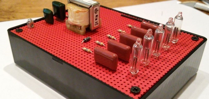
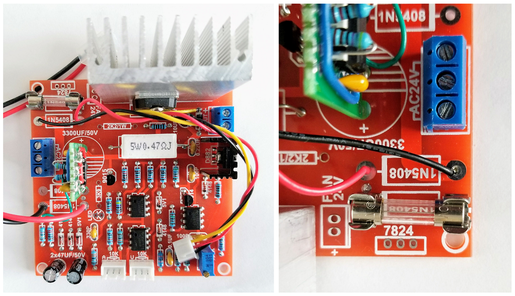
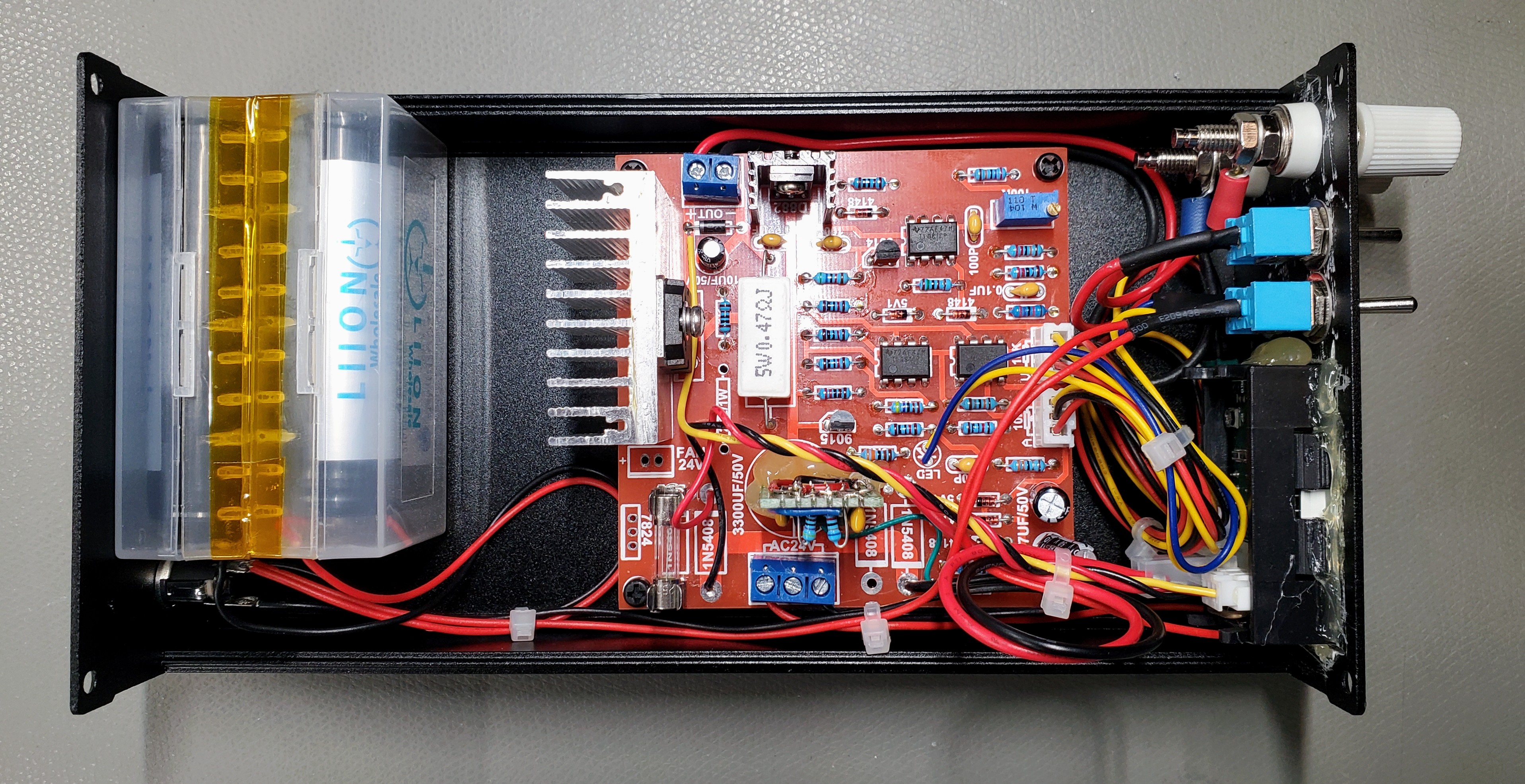
1. Battery Mod - Rectifier Circuit
To convert the Rectifier Circuit to battery operation, we first eliminate all of the components that aren't needed. This saves weight, reduces cost (i.e. unused parts can be used for another project), and makes space available for some new components.
The components that are not needed are:
- Rectifiers D1 through D4 (1N5408)
- Resistor R1 (2.2K 1W)
- Capacitor C1 (3300uF 50V)
Do not install the components listed above.
Optional Components are:
- Positive 24V Regulator IC U4 (7824)
- 2-pin Connector J5
- 24V 100mA Fan
I elected to skip the 24V regulator and fan as convection cooling would be sufficient for my purposes and the battery voltage will be too low to engage U4. If you think you'll need some extra cooling you will need to replace U4 with a Positive 12V regulator (Part Number 7812) and switch out the 24V fan with a 12V equivalent. Just about any 40mm X 40mm fan with a 2-Pin connector will work, or just solder in the fan leads. Just keep in mind that the fan will consume around 100mA which will shorten battery run-time. A simple electronic thermostat will help and would be a good design exercise for another time.
The components I added were:
- 2A Fast Blow Fuse (5mm X 20mm)
- Through-Hole Fuse Holder (5mm X 20mm)
- 555-based Astable Timer
- DROK V/I Panel Meter
In order to gain a bit more headroom on the -5V supply, I replaced the 5.6V zener D5 (1N752) with a 5.1V zener (1N751). This change is optional but recommended if you have the part on hand.
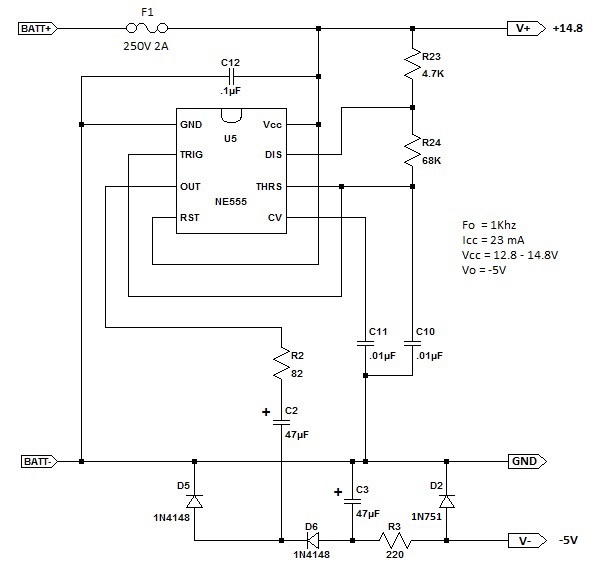
The changes made to the Rectifier Circuit are shown in the schematic above.
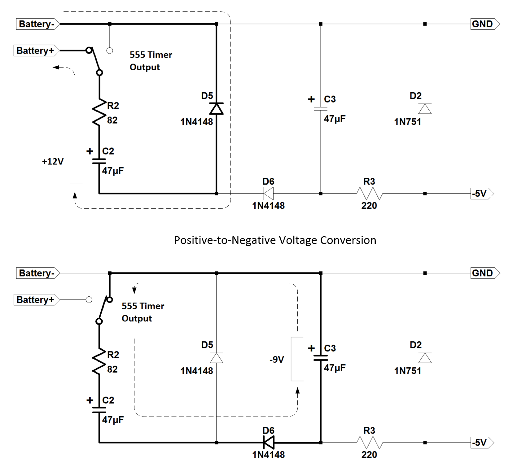
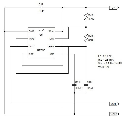
The 555 astable timer is used to replace the positive-to-negative charge switching done by the transformer and bridge rectifier. When the output of the 555 timer is high, capacitor C2 is charged to +12V through diode D5 and resistor R2, while capacitor C3 is discharging into the -5V regulator circuit. When the output of the 555 timer is low, R2 is shorted to ground which reverses the polarity of capacitor C2 and discharges C2 into capacitor C3 through resistor R2 and diode D6. C2 charges C3 to -9V with respect to ground before the cycle repeats. The resulting sawtooth voltage on capacitor C3 is regulated to -5.6V by R3 and Zener diode D2 and sent on to the function blocks that need -5V.
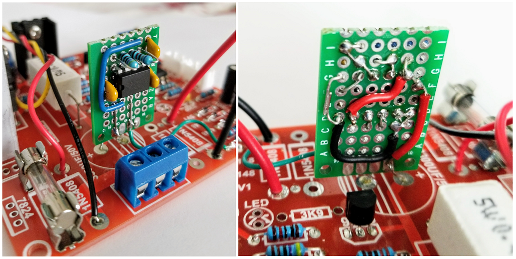
I built the Astable Timer (photos below) on a small piece of prototyping board using the following design procedure:
Most electrolytic capacitor manufacturers provide design data for 60Hz, 120Hz and 1000Hz, so I chose an astable frequency of 1Khz with near 50% duty cycle to minimize the ripple voltage in the converter.
I used the astable circuit from the datasheet and calculated the values for C24, R23 and R24 according to the equations:
T1 = 0.693 * ( R23 + R24 ) * C24 where T1 is the charge time for C24
T2 = 0.693 * R24 * C24 where T2 is the discharge time for C24
F = 1 / ( T1 + T2 ) where F is the astable frequency
DC = R24 / ( R23 + ( 2 * R24 )) where DC is the astable duty cycle
I wanted to keep current consumption on the astable timer low to keep battery drain to a minimum so the combined values of R23 and R24 need to be fairly large. TI includes a nice nomograph that shows the capacitor value needed for a certain frequency and resistor combination. I used that to choose a .01uF value for C24 because the combination of R23/R24 would be near 100K Ohms. Arranging the equation for T1 above to solve for R23/R24 and substituting known values gave:
R23 + R24 = T1 / ( 0.693 * C24) = .0005 / ( 0.693 * .00000001 ) = 72,150 Ohms
The .0005 term for T1 is the cycle time for 1000 Hz (.001 seconds) divided by two for charge time which makes T1 equal to .0005 seconds.
The astable schematic and duty cycle equation shows that a 50% duty cycle requires a large resistor value for R24 and a small resistor value for R23. However, R23 can not be so small that power dissipation in the 555 is exceeded. So I first selected the value for R24 by consulting the EIA E12 resistor chart which describes the most common resistor values I have in inventory, and looked for the resistor value closest to 72,150 Ohms without going over. That value was 68K Ohms. Subtracting 68000 Ohms from 72150 Ohms left 4150 Ohms for R23. Consulting EIA E12 again, I chose the closest resistor value above 4150 Ohms, which was 4.7K, and used that for R23.
Checking the resistor values with the equations shows:
T1 = 0.693 * ( R23 + R24 ) * C24 = 0.693 * ( 4700 + 68000 ) * .00000001 = .000504 seconds
T2 = 0.693 * R24 * C24 = 0.693 * 68000 * .00000001 = .000471 seconds
F = 1 / ( T1 + T2 ) = 1 / ( .000504 + .000471 ) = 1026 Hz
DC = R24 / ( R23 + ( 2 * R24 )) = 68000 / ( 4700 + ( 2 * 68000 )) = 0.48 or 48%
These results are almost perfect for the purpose. C11 and C12 in the schematic are bypass capacitors recommended in the 555 datasheet (attached below).
To prevent internal short circuits from damaging the battery, wiring, or circuit board components I recommend installing a Bussman 250V 2A fast acting fuse (5mm X 20mm, Part number GMA-2R) and fuse clips on the PCB as shown above. I used the pads for rectifier D1 to mount the fuse clips. Bussman recommends that the DC voltage applied to their fuses be no more than 1/2 the AC rating, or 125V, to ensure fast clearing of a fault. The maximum battery voltage of 16.8V is well below that. The cold DC resistance of the GMA-2R is 0.066 Ohms which is about the same is an equivalent automotive fuse. If you feel more comfortable using a purely DC rated fuse, feel free to substitute an automotive fuse for the glass fuse I used.
The DROK panel meter will be covered in a later step. The next step will cover the construction and installation of the astable timer.
The LM555 Datasheet is >>> HERE <<<
2. Battery Mod - Astable Timer Construction
The astable timer I built is constructed on a small piece of prototype board. You can use anything you have on hand and you can use any layout that works for you. Just follow the schematic diagram included above. I've included a top/bottom layout diagram below for the astable timer I built to use as a guide.
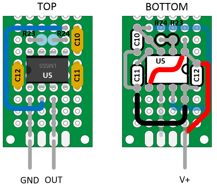
After the astable time is constructed, the trace connecting R2 to rectifier D4 must be cut in the location shown below. Then solder in the astable timer onto the traces indicated below. Small pieces of solid #22 or #24 hookup wire can be used for the V+ and GND leads when the astable timer is installed in the C1 position. But a 2" length of stranded #24 or smaller hookup wire will be needed for the OUT signal to reach R2.
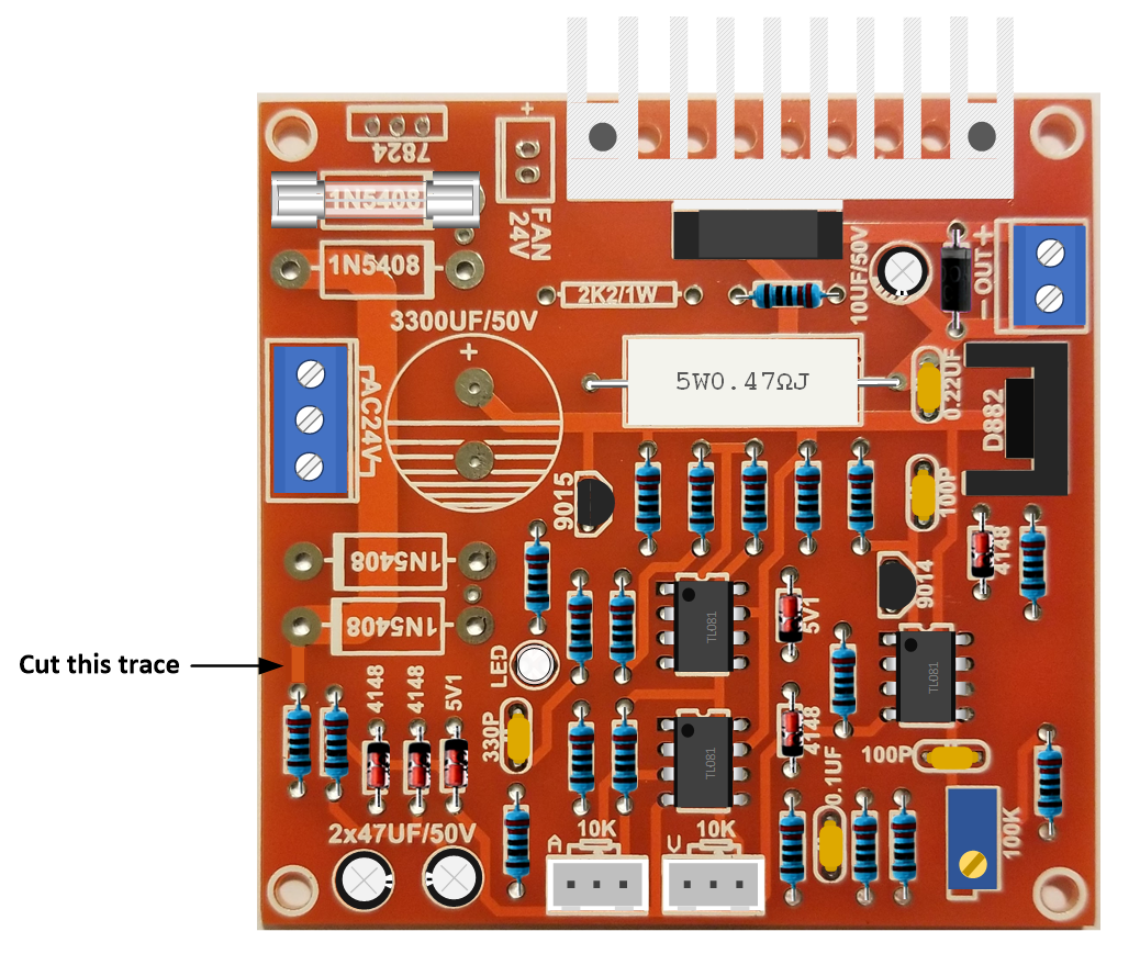
If you aren't planning on attaching a V/I panel meter to the power supply, solder in a #18 or larger jumper wire in the location shown below. Otherwise, install the DROK panel meter before testing the astable timer (see the Multi-Meter Mod in section 6 below).
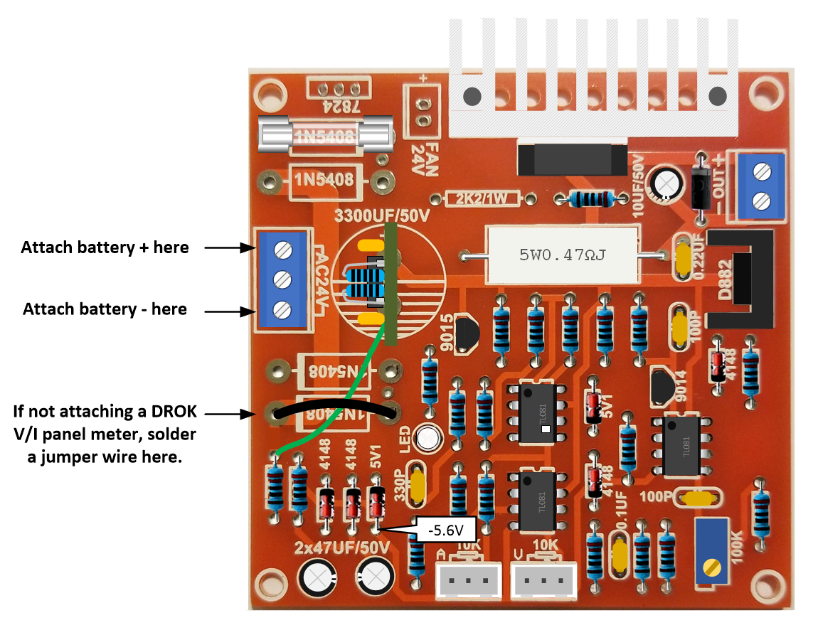
When completed, attach a 12V to 16V power source to J1 as indicated above. Check the voltage at the indicated test point to verify that the timer is working correctly.
3. Battery Mod - Reference Circuit
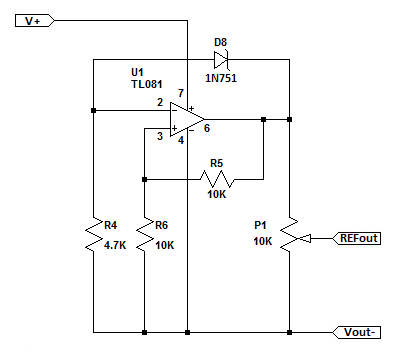
The minimum battery voltage for the 18650 pack I'll be using is 12V. The TL081 OpAmp IC saturation voltage is 1.5V below V+ which is not enough headroom for an 11.2V reference voltage. And I was not convinced that the 5.6V zener was the best choice for temperature compensation. So I elected to replace the 5.6V zener diode included in the WeiKedz kit with a 5.1V zener from my inventory. This will provide a 10.2V reference voltage which is just enough headroom as the battery pack reaches cutoff.
Replace D1 with a 5.1V zener part number 1N751
The 1N751 Datasheet is >>> HERE <<<
4. Battery Mod - Error Amplifier Circuit

The nominal battery voltage for the 18650 pack I'll be using is 14.8V. Accounting for TL081 saturation voltage (1.5V below V+) and the voltage drop in the power section (1.4V), the maximum output voltage is 11.9V. The gain of the Error Amplifier need to be changed to account for the different V+ voltages (13.8V on battery vs 32.5V on transformer power). Instead of a gain of 3, I needed a gain of:
Acl = Vout / Vref = 12V / 10V = 1.2
The non-inverting amplifier gain equation is:
Acl = 1 + ( R12 / R11 )
To avoid changing the frequency response of the Error Amplifier, resistor R12 should be left at 56K. Rearranging the gain equation to solve for R11:
R11 = R12 / ( Acl - 1 )
Substituting known values makes R11 equal to:
R11 = 56000 / ( 1.2 - 1 ) = 280,000 Ohms
The nearest IEA E12 resistor value is 270K Ohms.
Replace R11 (27K Ohm 1/4W) with a 270K Ohm 1/4W resistor.
For a reference input voltage between 0V and 10V, the power supply output voltage will vary between:
Vout = Acl * Vref
Vout = 1.2 * 0 = 0V
Vout = 1.2 * 10 = 12V
5. Battery Mod - Current Limiter Circuit
For my purposes I only wanted a maximum of 1A output current. But the current limit control is scaled for 0 to 3A which means that only the first 1/3 of potentiometer rotation would be useful, and if rotated further would allow a higher output current than desired. So the current limit scaling resistor R18 needs to be changed.
The voltage on the current sense resistor R7 depends on the power supply output current. The minimum current limit according to WeiKedz is 4mA and the maximum current for the battery modified power supply is 1A. So the voltage on R7 is:
V = I * R
Vlow = 0.004A * 0.47 Ohms = .002V
Vhigh = 1A * 0.47 Ohms = 0.47V
The output voltage of potentiometer P2 needs to vary between 2mV and 470mV.
If R17 is left at 33 Ohms and the voltage out of the Reference Circuit is 10.2V, then the value of R18 needs to be:
R18 = (( Vref / Vhigh ) - 1 ) * ( R17 + P2 ) = (( 10.2 / 0.47 ) - 1 ) * ( 33 + 10000 ) = 207,704 Ohms
The nearest EIA E12 resistor value is 200K Ohms.
Replace R18 with a 200K Ohm 1/4W resistor.
Using this value to check minimum current limit results in:
Iout = ( Vref * R17 ) / (( R17 + P2 + R18) * R7 )
Iout = ( 10.2 * 33 ) / (( 33 + 10000 + 200000 ) * 0.47 ) = .00034 or 3.4 mA
This is close enough to allow the power supply output current to be varied between 3mA and 1A.
6. Multimeter Mod - Adding a VI Display
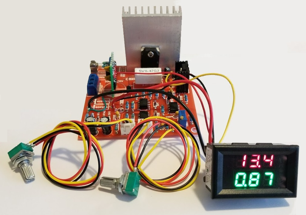
Adding a panel meter to the power supply is a simple matter of soldering in the power, voltage monitor, and current monitor leads at specific pads on the WeiKedz variable power supply PCB. I wanted both a voltage and current display. And I like the look of red/green/blue 7-segment LED's instead of the bland grey of LCD displays, and I didn't want to get too fancy with color LCD meters that measure a whole bunch of parameters. After looking around on Amazon, I liked the DROK V/I DC 0-100V 10A panel meter (Amazon ASIN B00EXCUHJU) best because it has an offset null and span adjustment for current measurements.
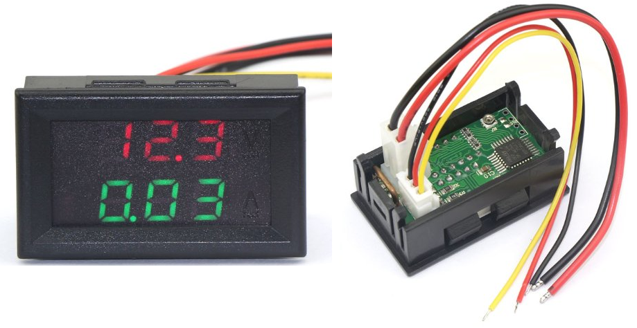
The documentation provided by DROK has not made much sense to me and doesn't appear to be accurate. For example, the documentation for the panel meter I bought suggests that the power leads are isolated from the voltage and current monitor leads. However that is not that case. The meter power ground and current monitor negative lead are internally connected together. And the voltage monitor lead is reference to the power ground lead. So the meter power supply is not electrically isolated from the power supply being monitored as shown in the documentation. Instead, the meter power, load voltage being monitored, and load current being monitored will share the same ground.
As it turns out, though, this panel meter is easy connect to the WeiKedz power supply and works great.
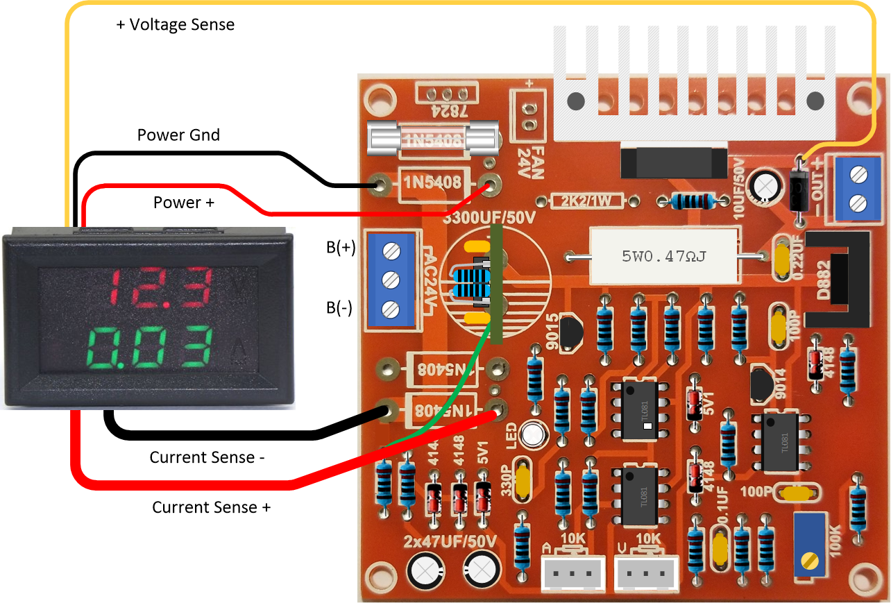
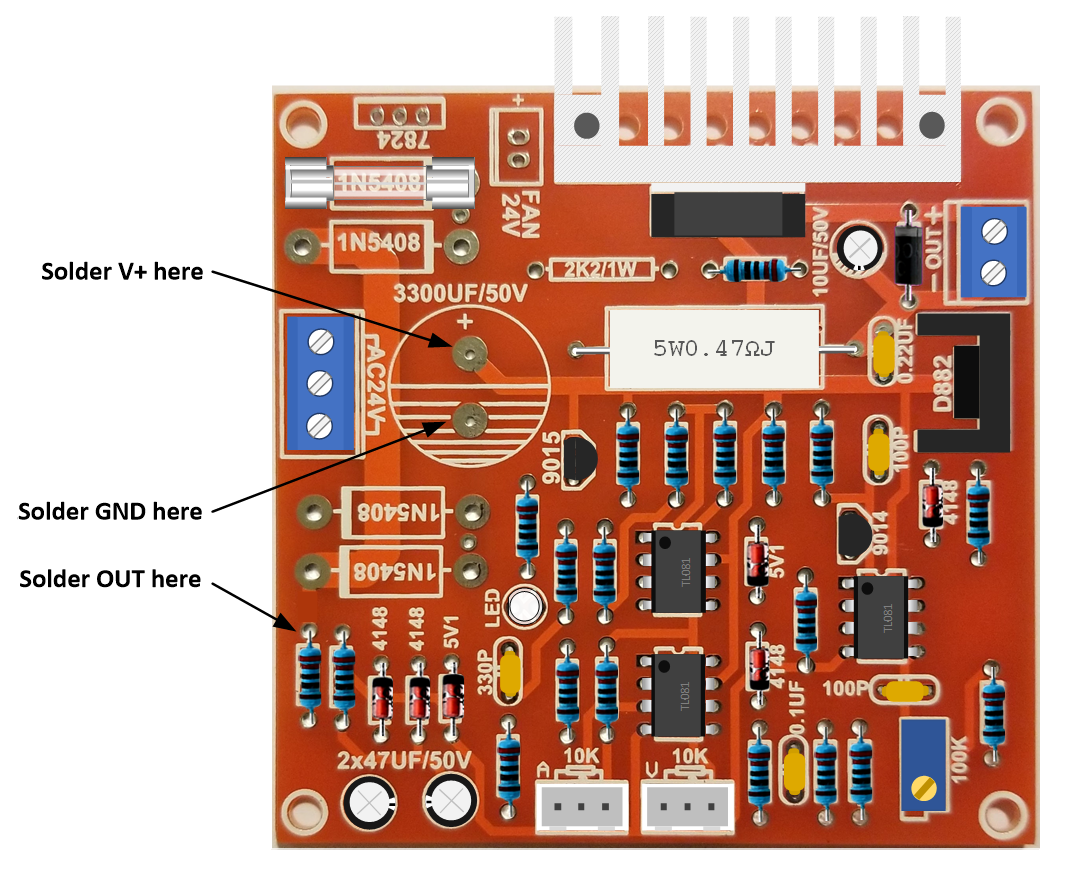
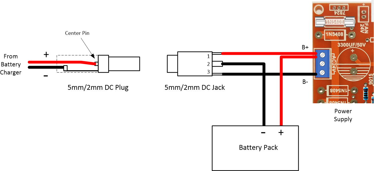
1. Solder the thin red meter lead to the battery + input PCB trace as indicated in the diagram above. The meter + lead will use the unoccupied PCB pad assigned to rectifier D2 cathode.
2. Solder the thin black meter lead to the battery - input PCB trace as indicated in the diagram above. The meter - lead will use the unoccupied PCB pad assigned to rectifier D2 anode.
3. Solder the thin yellow voltage monitor lead to the power supply + output PCB trace as indicated in the diagram above. The voltage monitor lead will be soldered directly to diode D11 cathode.
4. Solder the thick red current monitor + lead to the power supply GND trace as indicated in the diagram above. The current monitor + lead will use the unoccupied PCB pad assigned to rectifier D4 anode.
5. Solder the thick black current monitor - lead to the battery - input PCB trace as indicated in the diagram above. The current monitor - lead will use the unoccupied PCB pad assigned to rectifier D4 cathode.
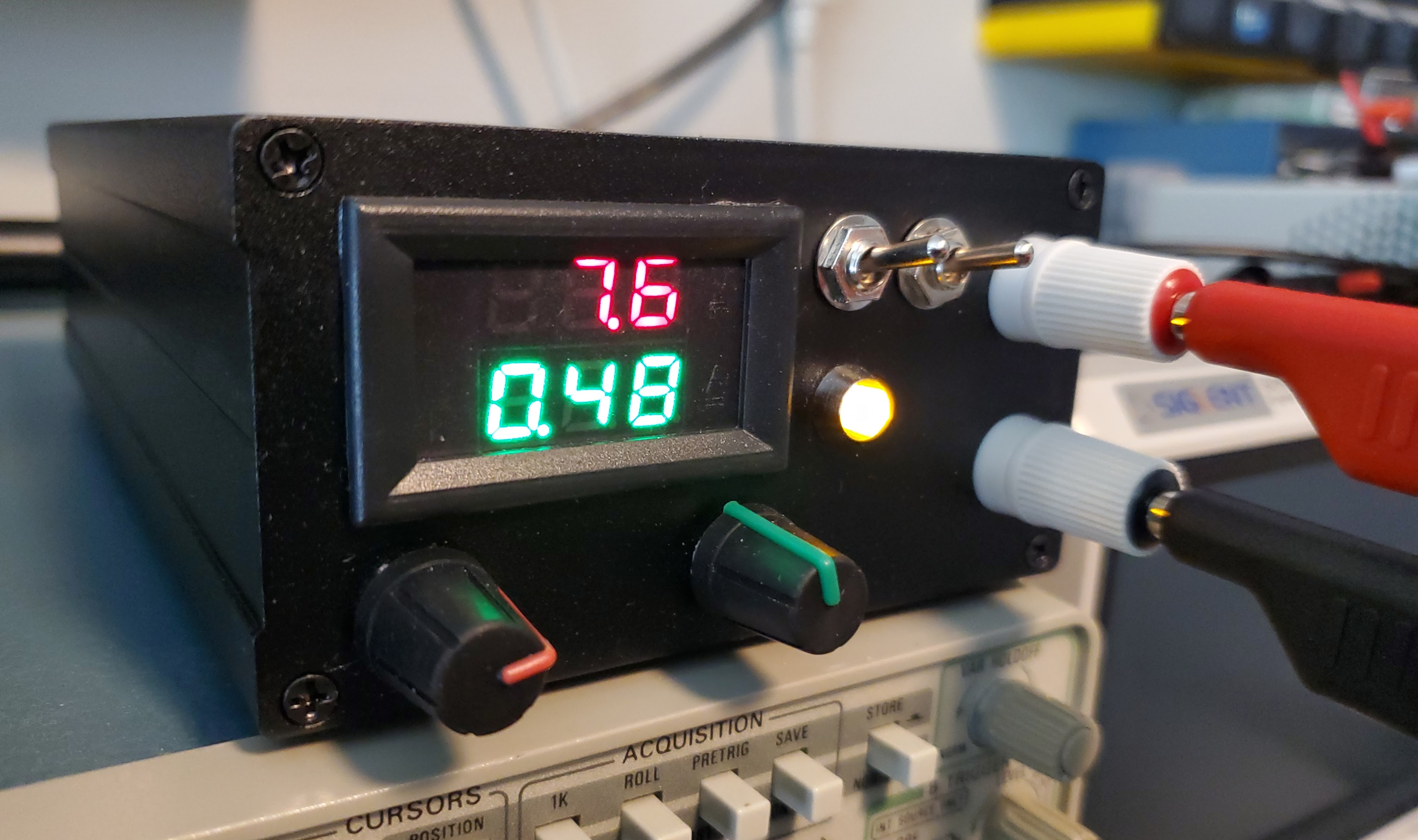
To test, verify that voltage potentiometer P1 is fully counter-clockwise and current potentiometer P2 is fully clockwise. Attach a 10 Ohm 10W load resistor to the power supply output. Attach a 14.8V battery positive lead to the B+ terminal on J1 and the battery negative lead to the B- terminal on J1. The panel meter will power on and display 0V/0A. Slowly rotate the voltage potentiometer clockwise and verify that the voltage and current measurements are close to the following:
Voltage Current
1.00 0.10
2.00 0.20
3.00 0.30
4.00 0.40
5.00 0.50
6.00 0.60
7.00 0.70
8.00 0.80
9.00 0.90
10.00 1.00
The DROK panel meter has a small trimmer resistor on the back that can be used to adjust the current measurement to more closely match the above table if needed.
7. Battery Charger
I installed the battery pack in a case with the power supply PCB. To charge the supply without having to disassemble the case each time I purchased a Tenergy TLP4000 Universal Li-ion/Li-Po battery charger from Amazon (ASIN B007MD54NQ). The "protected" cells I used contain their own internal charge/discharge controller so a separate balance circuit wasn't needed. If you use "unprotected" cells, you will need to purchase a balance charge/discharge PCB to avoid unfortunate accidents during use. You can use any battery charger you wish as long as it is designed for the 14.8V pack voltage.
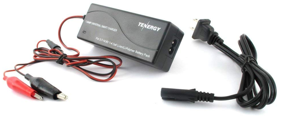
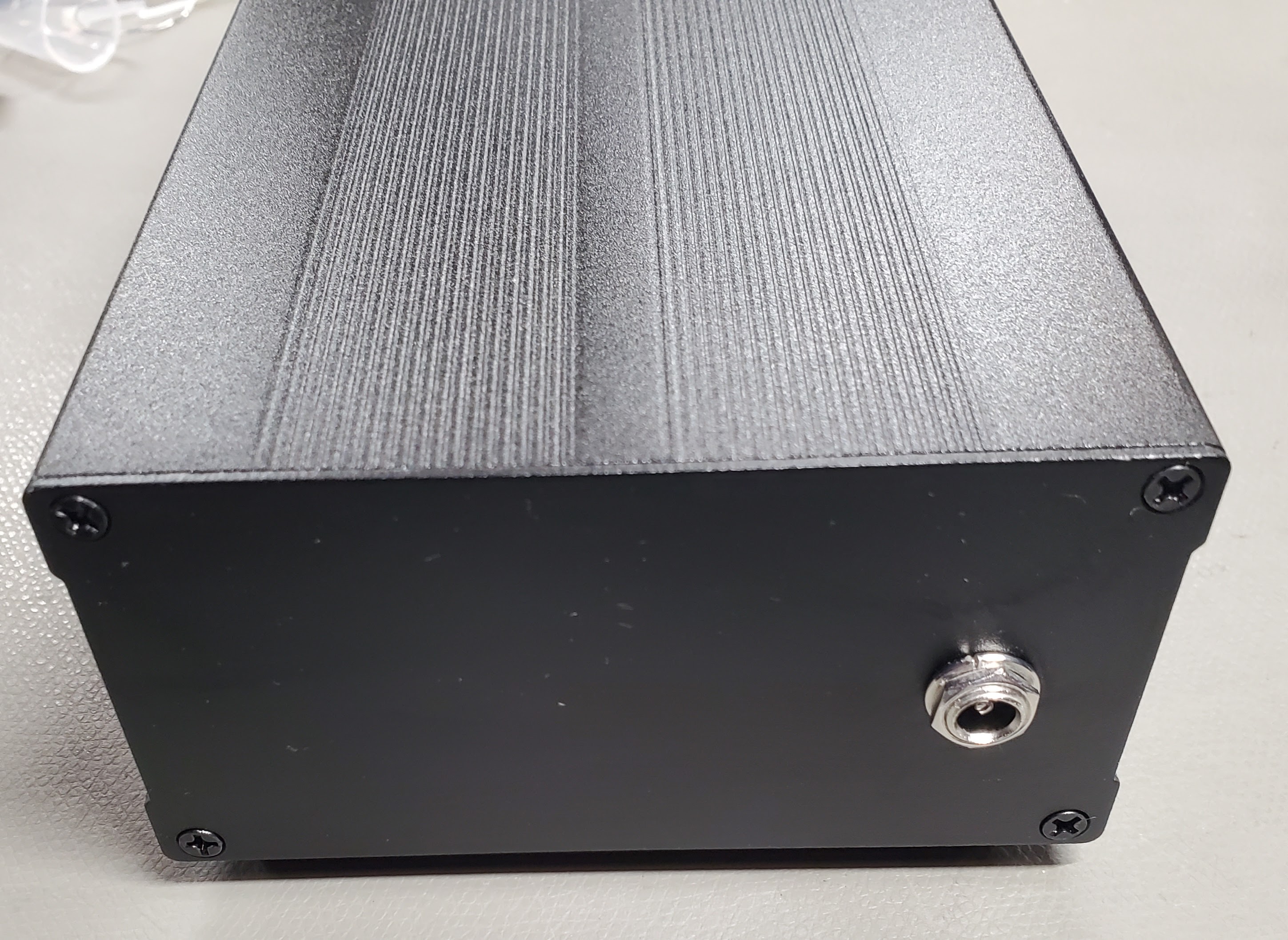
To connect the Tenergy charger to the power supply, I removed the alligator clips provided with the charger and soldered in a 5mm/2mm DC power plug (Mouser 490-PP3-002A) rated at 24VDC and 5A. Then I installed a panel mounted 5mm/2mm DC power jack (Mouser 490-PJ-005A) into the case. The DC input jack is a 3-wire type that disconnects the power supply from the batteries when charging. You can use any DC plug/jack you wish as long as the voltage rating is 24VDC and the current rating is 1A or higher. But be extra careful wiring the charging circuit so that charger, battery, and power supply get connected in the proper polarity is show in the illustration below. Be sure to check the manufacturers datasheet for the DC jack you use to make sure the battery and power supply connections are correct. Pins 1, 2, and 3 are different for each manufacturer. If in doubt, you can verify the pin-out with an Ohm meter. I've included the datasheet for the plug and jack I used below.
The DC Input Plug datasheet is >>> HERE <<<
The DC Input Jack datasheet is >>> HERE <<<
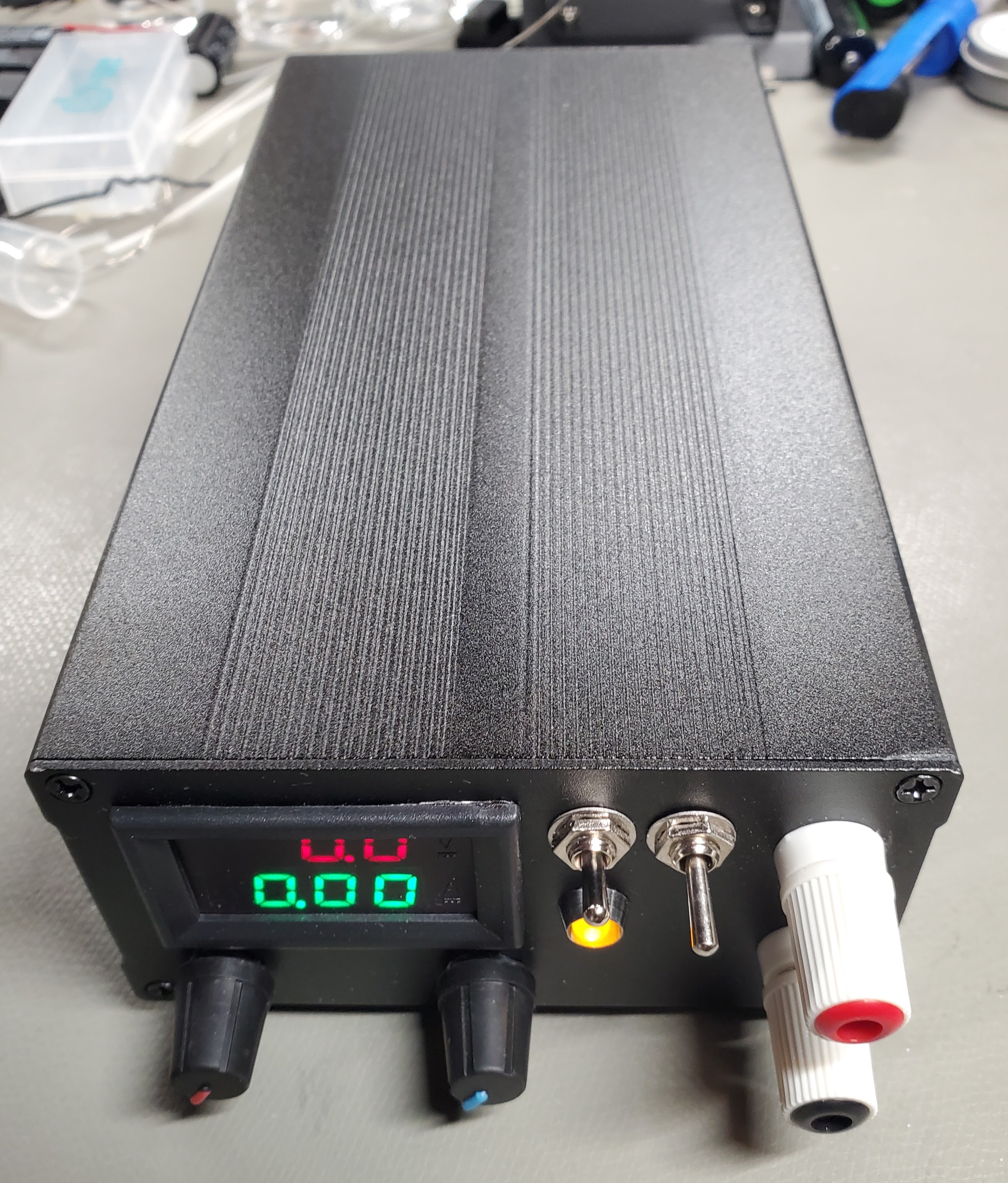
Put it in a case
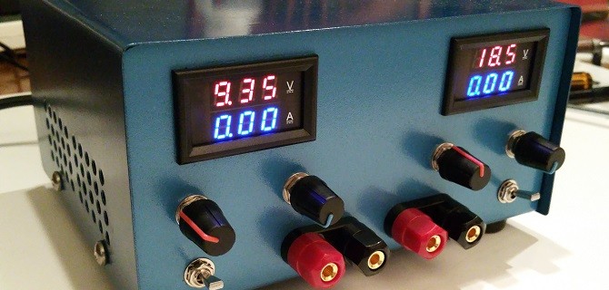
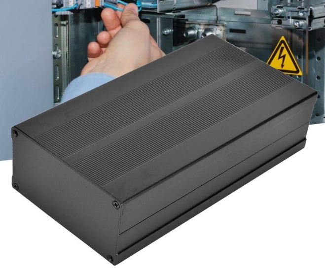
To make the portable power supply really useful it need to be in a safe enclosure. I was interested in a metal case for ruggedness having dimensions that would comfortably fit all the parts without a lot of wasted space. There are many options available on Amazon for not a lot of money. After some careful measurement and review I selected a black anodized aluminum case with dimensions 55mm X 106mm X 200mm. This turned out to be perfect for holding the battery pack, the regulator board, and the front panel controls. You'll find these offered by various sellers so check delivery and pick the best price as there is unlikely to be any difference in materials and finish.
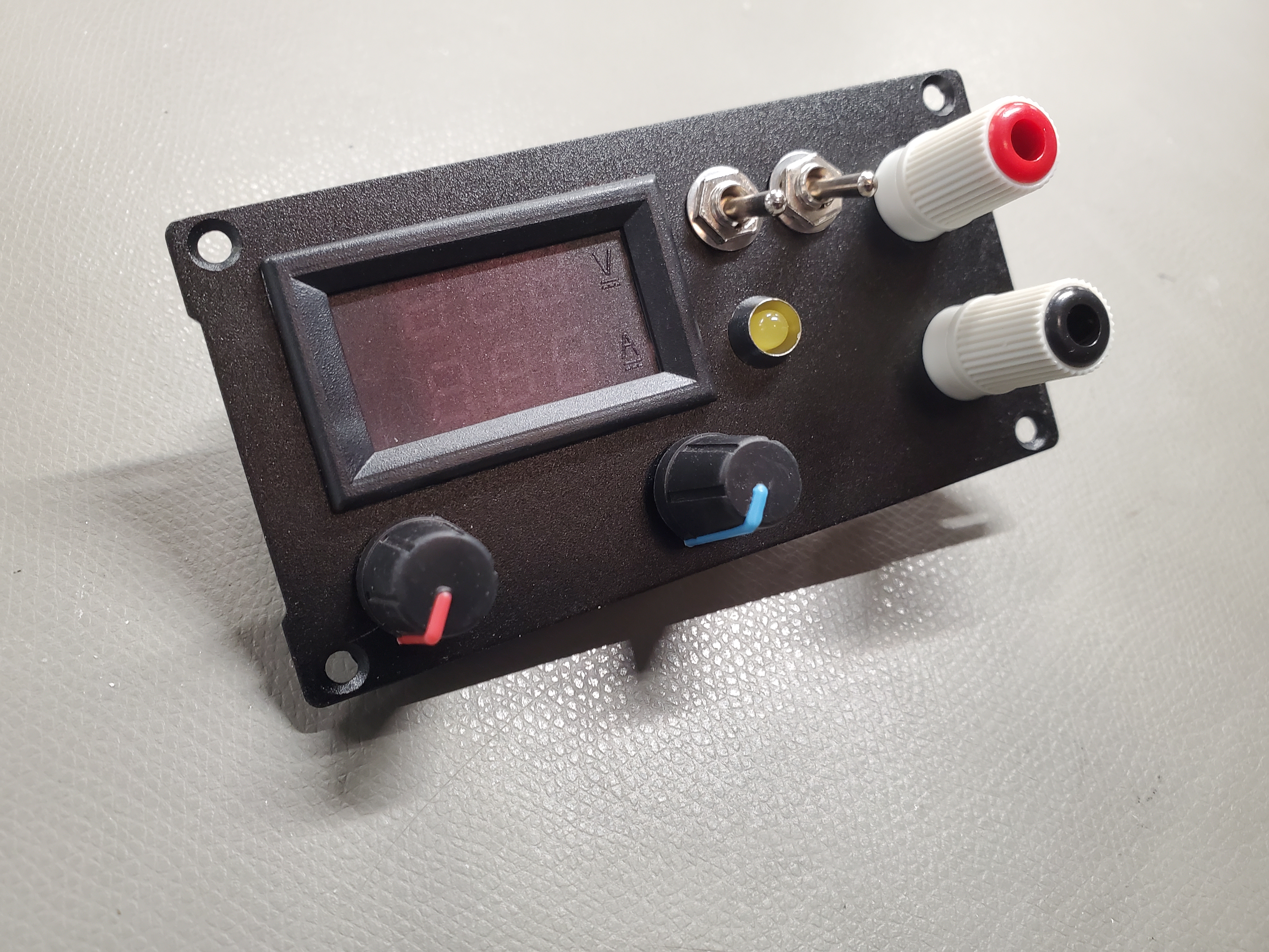
I mounted the V/I display on the front panel and added a battery power switch to turn the power supply on and off. The batteries will be automatically disconnected from the power supply when the charging adapter is inserted but there needs to be a method of disconnecting the batteries when not in use. I decided to add an output power switch so the power supply could be disconnected from the load when needed. And finally I removed the constant current LED from the board and mounted it on the front panel. I think the finished power supply looks very professional and is a welcome addition to my workbench. It has already come in handy on a radio project and a DC-DC converter project where isolation from electrical ground was critical.
I had to trim down the main heat sink to get it to fit. The heat sink originally provided by WeiKedz was not sufficient for the potential power dissipation when running low-voltage high-current from a transformer. But from a 14.8V battery pack the reduced heat sink will do the job. Some sellers do not include the heat sink so if you get one with your kit be sure to consider it a "suggestion" and do your own thermal resistance calculations to make sure you won't have heating problems in the case you choose. For the battery case, I used the plastic case that Liion Wholesale sent me with the batteries. It came in very handy.
Conclusion
The WeiKedz variable power supply is a good kit that includes a good collection of parts for experimenting, including a large heatsink, fan, and regulator IC. The circuit is well designed and only suffers from voltage and current specifications that are two optimistic. When operated within realistic parameters, the power supply performs extremely well. It comes as a kit which is excellent for hacking. And for $10, the kit is a really good value. I now have a near silent variable power supply that is perfect for sensitive radio and instrumentation circuits. No 120 Hz ripple like you get with a transformer fed power supply. No 70KHz to 100 KHz hash like you get from these cheap switching power supplies. Just clean, smooth, stable DC that's electrically isolated from everything else around.
If you've stuck with me this far, I hope the information presented has been helpful.
Good Luck!
NetZener
Portable Variable Power Supply - Part 1
I'm working on a project that requires a portable battery-fed power supply that provides variable output voltage and an adjustable current limit. I needed an output voltage between 0 and 12V, current limit between 10mA and 1A, and load regulation 0.1% or better at full output voltage and current. Because the supply would be used in noise sensitive analog circuit design, I couldn't use one of the many switching regulator options available due to the 100mV of high frequency noise that's typical of those products.
The well-known LM317 is an easy way to meet my variable voltage requirement but constant current control isn't its strength. And its minimum output voltage is around 1.25V. Not a major issue but I would prefer to be able to drop the supply voltage to 0V when needed instead of having to flip a switch.
Before starting a custom design I thought I'd see what was available off-the-shelf, preferably in a DIY kit form so I would have some options on component values and controls placement. One product that consistently appeared on Amazon and eBay was the power supply kit featured in this article. The cost of the kit was so cheap I ordered two without doing further research. After receiving the kit I was impressed with the quality of the packaging, circuit board, and the variety of components included. Whatever the outcome, this kit was definitely worth the price.
After reviewing the documentation available on the Internet, the following phrase in bold letters caused some concern: "The circuit must be connected to 24V alternating current power, and direct current is forbidden". A quick look at the schematic told me why. The current limiter, error amplifier, and current pass depends on an -5V auxiliary supply derived from the main bridge rectifier. After thinking about the problem a few minutes the solution was obvious and is covered in Part 2 of this article. I've found an analog variable power supply kit that, with some modifications, fit my requirement exactly.
Introduction to the WeiKedz Variable Power Supply DIY Kit
Introduction
The WeiKedz Variable Power Supply DIY kit is an electronics project kit containing all the components needed to build an analog variable power supply EXCEPT transformer, power cord, knobs, and enclosure (more on this later). There are a number of distributors in Asia offering this kit under various brand names. But as of November, 2017 the WeiKedz branded version was available on Amazon (ASIN B01KNSCDNU) with Prime shipping for $14, which in my opinion is a great value considering WeiKidz includes a large aluminum heat sink, 24V fan, and mounting hardware.
The specifications for the power supply are as follows:
Input voltage: 24VAC
Input current: 3A (maximum)
Output voltage: 0-30VDC (adjustable)
Output current: 2mA to 3A (adjustable)
Output voltage ripple: maximum 0.01%
As you will see in the analysis sections that follow, these specifications are too optimistic. The power supply I assembled works very well and is suitable for almost any analog project the beginner or experienced maker is likely to find exciting. But it is not, by design, capable of achieving exactly these specifications. In addition, I ended up substituting a 20VAC transformer (Hammond 185F20) for the 24VAC transformer specified in the documentation in order to keep OpAmp supply voltages below the manufacturers maximum ratings. There is some assembly documentation available on the Internet, but it is hard to find and has some technical and English language weaknesses that I've corrected in the assembly document attached below. That being said, for $14 and the cost of a transformer it's a great kit that is fun to build. A V/I multimeter can be added to make it easier to set the output voltage and current limit.
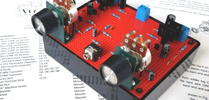
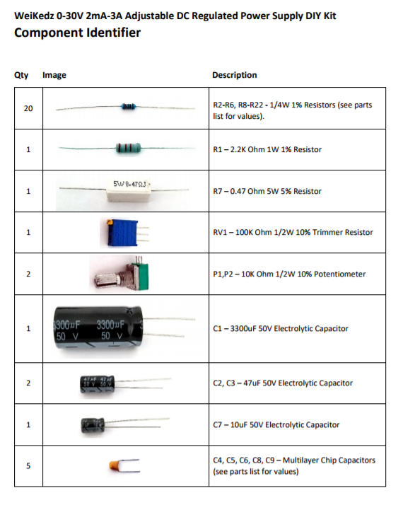
Parts List and Component Identifier
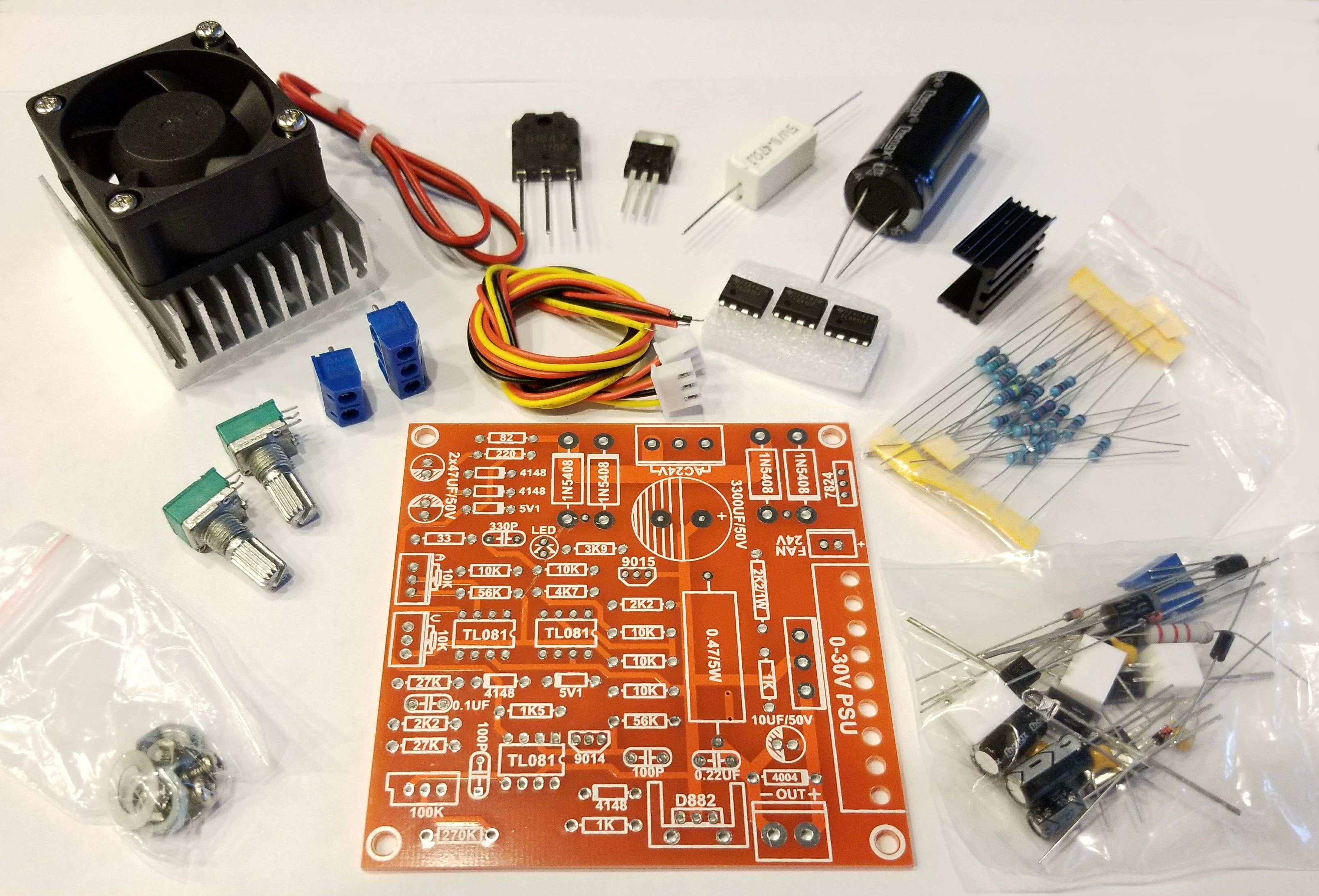
Attached below are the parts list and component identifier documents describing everything that came with my kit. For those new to electronics, the component identifier document will help you figure out which part is which. For some reason the manufacturers web site shows components that look like somebody stuffed them in their jeans and accidentally ran them through the wash. Never fear, all of the parts I received were well packed, protected where needed, and with clean and straight leads. So yours should arrive that way too.
Download the Parts List document >>> HERE <<<
Download the Component Identifier document >>> HERE <<<
Assembly Manual
If you should decide to build the WeiKedz power supply, I've also included a comprehensive assembly guide below that is a bit more detailed than that provided by the manufacturer. If you are new to electronics but have some experience with a soldering iron, this guide will provide just about everything you need to know to successfully build the kit.
Download the Assembly Manual >>> HERE <<<
Operation and Maintenance Guide
One of the weaknesses in the manufacturing design of the circuit board was the decision to use component values (100K, 4004, 5V1, etc.) on the component layer silk screen instead of schematic reference numbers (R1, C2, Q4, etc). The decision to use component values helps an experienced builder solder parts to the board with minimal documentation. But if you ever need to troubleshoot the power supply using the circuit diagram you are out of luck. The lack of reference numbers on the board makes matching a node on the schematic with the corresponding node on the circuit board very, very difficult. For example, there are five 10K Ohm resistors on the circuit board. Without a schematic reference number on the board, you can't tell which 10K resistor on the board goes with which 10K Ohm resistor on the schematic. All of the documentation I've included uses both component values and schematic references. The Operation and Maintenance guide contains images of the board along with it's components, component values, and schematic reference numbers. It also contains the tune-up procedures and some troubleshooting steps to follow if the power supply doesn't work properly. You will find this guide invaluable to maintaining the power supply.
Download the Operations and Maintenance Guide >>> HERE <<<
Circuit Analysis
In the next few sections, I'll break the power supply schematic down into it's major functional blocks and describe how each works and what most of the components do. This will help in determining how to make changes and substitutions that tailor the power supply for a specific application. For example, WeiKedz and other brands offering this kit for sale are not very specific on the transformer needed, which has been a source of most of the confusion builders have had with the kit. I'll clear that right up and show you how to make the proper selection based on your voltage and current requirements.
Hacking It
At the end of this article, I'll describe the changes needed to convert the power supply to portable (i.e. battery) operation and add a V/I display. This is the version shown on the cover. As you will see later, it's not as simple as attaching a battery with the correct voltage.
A note on content
Where possible I've attempted to describe the operation of various circuits using basic mathematics. The majority of electronic design can be done with a good understanding of algebra and a little bit of trigonometry (occasionally pressing the sin or cos button). Electronics concepts and some experience with the usual fundamental equations like Ohms Law, RC time constants, power factor, etc. is necessary. But I'm more interested in communicating the importance of one skill in particular: The ability to observe a physical system in action, write an equation that describes what is being observed, and use that equation to predict what will happen when the system is changed. THAT is a far more useful skill than just memorizing the laws of exponents. Designing and then building a working circuit is way more fun and satisfying than blindly plugging in one resistor or capacitor value after another until it works. I know some folks who are pretty good at doing things that way, but they are more interested in the art of the thing than the science.
Special Note: I have no business relationship with any vendor mentioned in this article. Nothing of financial value was exchanged for my recommendation. None of the vendors mentioned in this article provided compensation of any kind during the creation of this project. I will not be compensated in any way if you choose to build this project or purchase components from any vendor I recommend. I simply had a good experience with the vendors I recommend and believe you will too.
Power Supply Block Diagram and Schematic Diagram
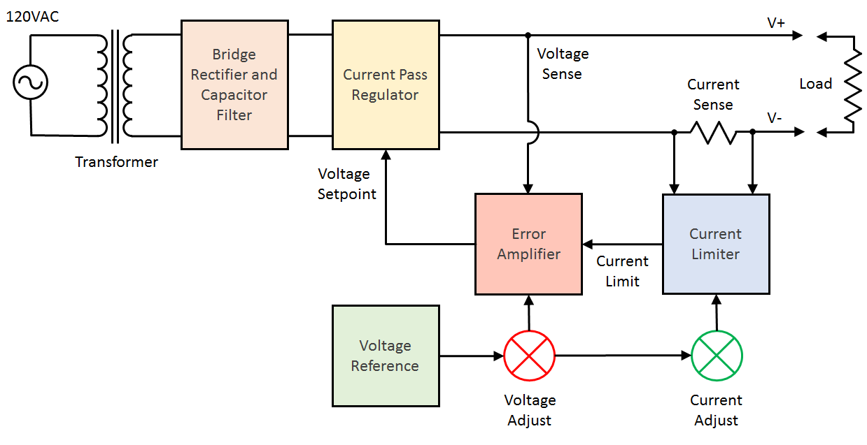
The WeiKedz variable power supply is a fairly standard design with 5 functional blocks as described below:
Bridge Rectifier and Capacitor Filter
Converts the 24 VAC power from the transformer into +32.5 VDC and -5 VDC power for use by other function blocks.
Voltage Reference
This is the heart of the power supply. It's job is to provide a fixed known reference voltage that other function blocks use to control the power supply output voltage and limit the power supply output current.
Error Amplifier
This function works much like the thermostat in your home. You set the temperature you want, the thermostat compares that to the actual indoor temperature, and then signals the climate control system raise or lower the indoor temperature to match. The error amplifier works the same way. You set the output voltage you want, the error amplifier compares that to the actual output voltage and signals the Current Pass function to raise or lower the output voltage to match.
Current Limiter
This function works in similar fashion to the Error Amplifier except that it senses the output current (as opposed to the output voltage) and signals the Error Amplifier to reduce the output voltage when the current limit is exceeded. This helps prevent damage to the components of a circuit caused by wiring or design error.
Current Pass Regulator
This is the workhorse of the power supply. It's job is to maintain the voltage set by the Error Amplifier independent of the current drawn by the circuit attached to the power supply. During normal operation the power consumed by the circuit attached to the power supply will be less than the output power of the Bridge Rectifier/Filter function. This difference in power has to be consumed by the Current Pass Regulator and released as heat, which is why this function has large metal heat sinks attached.
Summary
I've attached a PDF version of the schematic for the WeiKedz variable power supply below along with the voltages that will appear when a 24 VAC transformer is attached. Each of the function blocks above is described in detail in the steps that follow.
Download the Power Supply Schematic >>> HERE <<<
Problems With the WeiKedz Power Supply Design
Before I start the analysis I'd like to mention that the manufacturers specifications for the power supply are far too aggressive.
This is not a power supply capable of reliably delivering 0-30VDC at 0-3A. The power supply I assembled was unable to achieve the manufacturers specifications for all voltage and currents. For example, I experienced overheating in capacitor C1 and transistor Q4 when drawing 3 Amps from a 5V output setting which would have resulted in the catastrophic failure of these components had I allowed the test to run uninterrupted. You'll see why in the sections that follow.
Below is the short list of issues with the design:
1. Transformer VI recommendation is under-sized.
2. Ripple current for C1 exceeds manufacturers maximum ratings when output current >1A.
3. Power supply range (V+ and V-) exceeds manufacturers maximum ratings for U2 and U3 (TL081).
4. Vceo for Q2 (2SD882) exceeds manufacturers maximum rating when output voltage is 0.
5. Ripple voltage for C1 exceeds regulation window for 30V at output current >100mA
The above issues will result in near-term component failure after the power supply is placed in service.
However, I think the power supply is a good design that has simply been over-specified. Below are my recommendations for how the power supply should be operated for good long-term reliability if no component substitutions are made:
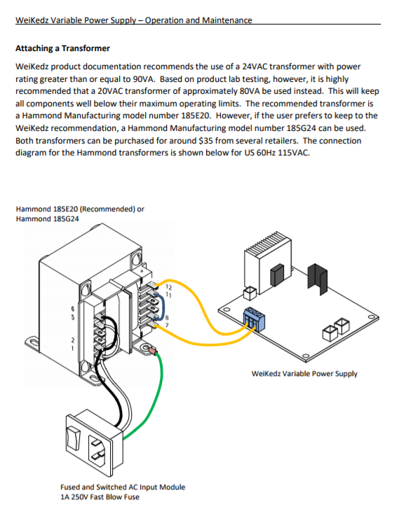
Transformer: 20V RMS @ 4A (Hammond 185E20)
Output Voltage: 0-20V
Output Current: 0-1A
With the above ratings, the fan can be omitted and the large heat sink on Q4 can be reduced in size (I cut mine almost in half). The transformer sizing I've specified covers you for the low power factor of the secondary current and allows for +/- 10% line voltage tolerance at the mains. And, the full 1A current can be drawn from any output voltage setting.
1. Analysis - Rectifier and Filter Circuit
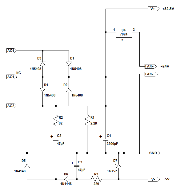
If you examine the schematic diagram above, you will notice that there are three power supplies associated with this function block: The V+ Supply, the V- Supply, and the Fan Supply. A short description of each is provided below followed by a more detailed operating analysis.
Description: The V+ Supply
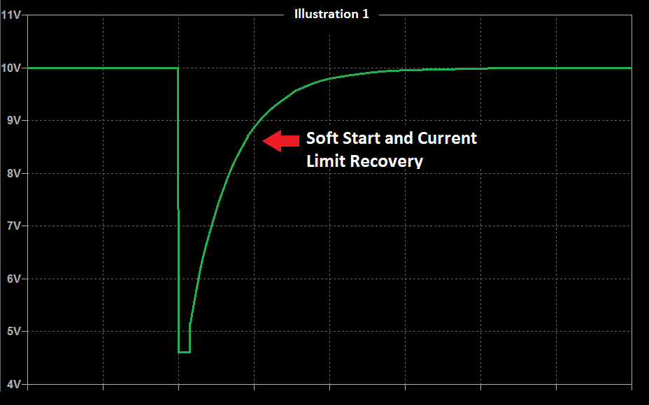
The rectifier and filter section is a very basic full-wave bridge circuit (D1 through D4) with a large filter capacitor attached (C1). Resistor R1 will safely discharge C1 when AC power is disconnected from the transformer. Regulator U4 drops the V+ voltage to 24V to power the cooling fan provided in the kit. The transformer attached to the power supply provides an alternating current (AC) voltage with frequency of 50Hz or 60Hz depending on country. On the positive half of the AC cycle, diodes D1 and D4 conduct which charges capacitor C1 for that portion of the cycle. On the negative half of the AC cycle, diodes D2 and D3 conduct which also charges capacitor C1 for that portion of the cycle. See Illustration 1 below.
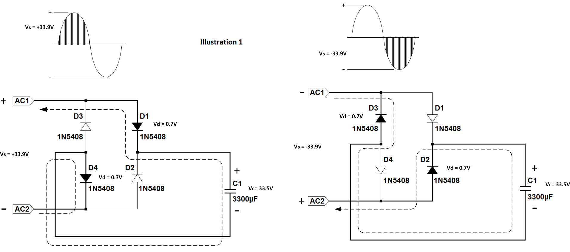
Description: The V- Supply
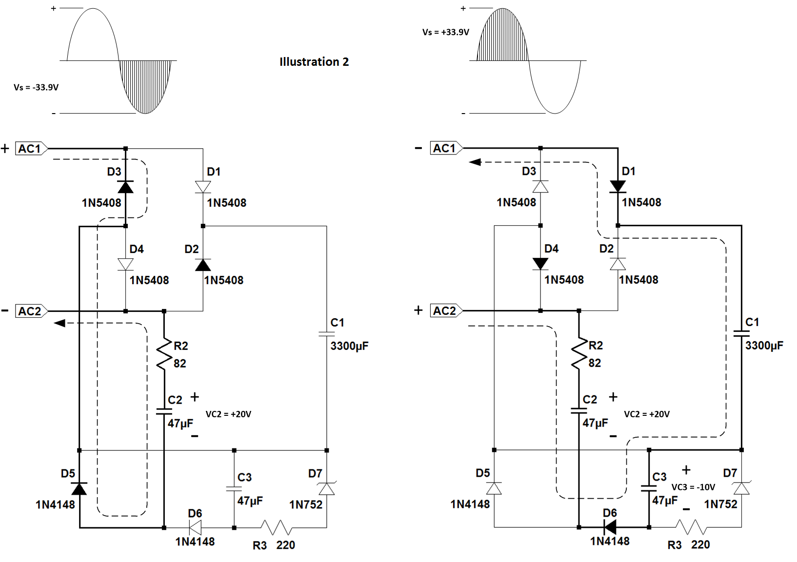
The remainder of the circuit is a -5V power supply for use by the Current Limit, Error Amplifier, and Current Pass function blocks. During the negative half of the AC cycle, C2 is charged through R2 and D3/D5. The time constant of R2/C2 allows C2 to reach an average charge of about +21.5V. R2 also serves to limit the ripple current in C2 to around 60mA which is important as the manufacturers datasheet recommends no more than about 112mA ripple current or reliability will be affected. During the positive half of the AC cycle, C2 discharges into C3 via R2 and D1/D6 until C3 reaches an average charge around -10V. Zener diode D7 then regulates the voltage from C3 down to -5.6V which is then sent to other power supply function blocks. For this supply to work correctly, the transformer must have a secondary voltage of at least 18V RMS. See Illustration 2 below.
Description: The Fan Supply
The fan included with the WeiKedz power supply is a standard DC brushless fan requiring 24V at 100mA. A three-terminal regulator IC U4 (7824) is used to provide a constant 24V output to the fan. Power dissipation for U4 is almost 1W so this part will get very warm during operation. There is no heat sink provided for this part so some convection or forced air flow will be required to keep it from going into thermal shutdown.
Function Block Analysis
Let's take a close look at the components involved and examine a few formula that describe the operation of this portion of the circuit:
A. Surge Current
When the power supply is first turned on, the bridge circuit will see a very large current spike during the first half AC cycle. This "surge current" is the result of charging capacitor C1 from it's initial voltage at or near 0. The magnitude of the surge current depends on the series DC resistance of the transformer secondary winding, the effective series resistance of capacitor C1, the initial voltage of capacitor C1, and the transformer voltage at the time the power supply was turned on. Non-repetitive surge current will not produce enough heat to damage the transformer or C1, but excessive surge current can instantly destroy rectifiers D1 through D4. According to the 1N5408 datasheet, the maximum surge current for one half cycle is 200A. During testing with a suitably sized transformer (Hammond 185G24), the power supply I built produced a surge current of around 40A which is well within the margin of safety.
RESULT: Surge Current performance is ACCEPTABLE
B. V+ and V- Supplies
With no load attached to the power supply, capacitor C1 will charge very quickly to the peak voltage described by the formula below:
V+ = (Transformer Vrms * 1.414) - 1.4
V- = -5.6V (For transformer secondary >= 18V RMS)
So if you do what WeiKedz recommends and attach a 24V RMS transformer to the power supply, both power supplies will reach the following voltages:
V+ = (24 * 1.414) - 1.4 = 32.5V
V- = -5.6V
The total range for both supplies is 38.1V. This is the first problem with the design specifications. There are two integrated circuits, U2 and U3 (TL081), that are connected to both supplies. However the manufacturers datasheet for the TL081 specifies the absolute maximum supply range to be 36V. The recommended supply range for the TL081 is 30V. The manufacturer specifically states that operation outside of the recommended voltage range is not guaranteed and reliability is compromised when absolute maximum ratings are exceeded. For this reason, I do not recommend using a 24V RMS transformer for the WeiKedz power supply.
RESULT: V+ and V- Supply performance is NOT ACCEPTABLE
C. Ripple Voltage and Ripple Current
The peak to peak ripple voltage occurring across capacitor C1 when loaded is approximated by the following formula:
Vripple = I / (2 * f * C) where I is the load current, f is the mains frequency, and C is the value of C1 in Farads.
Ripple is important because it causes heating within the capacitor. The lifespan of a large electrolytic capacitor can be drastically shortened by internal heating due to electrolyte evaporation, can swelling, seal failure, and in extreme conditions explosive failure of the capacitor. For the WeiKedz power supply, the ripple voltage across C1 when the power supply is delivering 3A output current is:
Vripple = 3 / (2 * 60 * .0033) = 7.57V peak to peak
The equation result is an approximation due to the complexity of the actual charge and discharge waveforms on C1. In the power supply I built, the measured ripple voltage was approximately 6V peak to peak while operating at 3A output current.
Due to the many different sizes and voltage ratings of capacitors, manufacturers specify the maximum ripple rating as ripple current in mA. The formulas for determining ripple current in C1 is:
Iripple peak-to-peak = Vripple / sqrt(Xc^2 + ESR^2)
Iripple RMS = Iripple peak-to-peak / (2 * sqrt(3))
Xc = 1 / (4 * pi * f * C) where f is the mains frequency in Hertz and C is the value of C1 in Farads
ESR = DF * Xc where DF is the Dissipation Factor specified by the manufacturer and Xc is reactance of C1
The manufacturers datasheet for C1 indicates that DF is 0.12 and the maximum ripple current is 1.5A RMS. Solving each equation reveals:
Xc = 1 / (4 * pi * 60 * .0033) = 0.402 Ohms
ESR = 0.12 * 0.402 = 0.048 Ohms
Iripple = 7.57 / sqrt(.402^2 + 0.0408^2) = 18.74A peak to peak
Converting the Iripple value from peak-to-peak to RMS results in:
Iripple RMS = 18.74 / (2*sqrt(3)) = 5.4A which is far greater than the manufacturers specifications of 1.5A.
The above calculations show that regardless of output voltage, the power supply cannot deliver 3A without rapid heating and eventual destruction of C1. My actual measurements for ripple current in C1 were almost 4A and the temperature of C1 exceeded 60DegC in a matter of minutes. The best I could achieve without excessive C1 heating was 1A. This is the second problem with the power supply design specifications.
In addition, the ripple voltage on C1 at 3A output current results in the input voltage to the Current Pass function block (Vin) dropping below the 30V output specification (Vout):
Vin = (V+) - Vripple = 32.5V - 7.57V = 24.94V
Since Vin to the Current Pass function block must be greater than or equal to (Vout + 1.4), it is not possible for the power supply to produce a 30V DC output voltage (Vout) when the load current is 3A. The best I could achieve was a DC voltage of about 26V superimposed with a 6Vpp 120 Hz ripple voltage. Not good. This is the third problem with the power supply design specifications.
RESULT: Ripple Voltage and Current NOT ACCEPTABLE
D. Bridge Rectifier Peak Inverse Voltage and Average Forward Current
The two most important parameters for the rectifiers in the bridge section is Peak Inverse Voltage (PIV) and Average Forward Current (IFavg). PIV is the maximum voltage that can be placed across a rectifier in the non-conducting direction. Exceeding this specification can cause the diode to short circuit and burn out, a condition called avalanche breakdown. IFavg is the maximum average current that the rectifier can carry in the conducting direction. Exceeding this specification can cause the diode to overheat and burn out, a condition called junction thermal breakdown.
In a full-wave bridge rectifier, the maximum reverse voltage is equivalent to the transformer secondary peak voltage less one diode voltage drop. The formula for this is:
PIV = ( Transformer Vrms * 1.414 ) - 0.7
If you accept the WeiKedz specification and attach a 24V RMS transformer to the power supply the bridge rectifier PIV voltage will be:
PIV = ( 24 * 1.414 ) - 0.7 = 33.24V
The datasheet for the 1N5408 rectifier indicated that PIV should be no more than 1000V so there is no problem here.
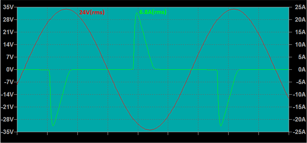
The datasheet specifies that the maximum average forward current can be no more than 3A. In a bridge rectifier configuration, each diode conducts 1/2 of the average current drawn by the load and filter capacitors. In a well designed full-wave bridge circuit, the rectifier current when conducting will be a very large but very short pulse (See Illustration 3). This pulse represents the energy needed to charge the filter capacitor back to peak voltage while powering the load at the same time. Because the pulse usually lasts less than 2ms of a 16ms rectifier conduction cycle, the rectifier current averaged over the entire 16ms cycle will be much lower than the peak current. In the WeiKedz power supply, the Average and Peak current while the bridge rectifiers are conducting is approximated by the following equations:
Iavg = I * ( 1 + pi * ( sqrt ( 2 * Vp / ( Vp - Vr )))) Where I is the Load Current in Amps, Vp is C1 peak voltage, and Vr is C1 ripple voltage.
Ipeak = I * ( 1 + 2 * pi * ( sqrt ( 2 * Vp / ( Vp - Vr )))) Where I is the Load Current in Amps, Vp is C1 peak voltage, and Vr is C1 ripple voltage.
Rectifier conduction time is approximated by the equation:
Dct = [ sqrt ( 2 * ( Vp - Vr ) / Vp ) ] / ( 2 * pi * 120 ) Where Vp is C1 peak voltage and Vr is C1 ripple voltage.
And the Rectifier Average Forward Current for an entire cycle is:
IFavg = Iavg * Dct * 60
Solving these equations for the maximum specified output current of 3A then gives a good estimate of the expected IFavg for rectifiers D1 through D4:
Iavg = 3 * ( 1 + pi * (sqrt ( 2 * 32.5 / ( 32.5 - 7.57 )))) = 18.22A
Ipeak = 3 * (1 + 2 * pi * (sqrt ( 2 * 32.5 / ( 32.5 - 7.57 )))) = 32.44A
Dct = [ sqrt ( 2 * ( 32.5 - 7.57) / 32.5) ] / ( 2 * pi * 60) = .0016 seconds
IFavg = 18.22A * .0016 * 60 = 1.75A
According to the 1N5408 datasheet this current is good for an ambient temperature up to about 90 DegC (194 DegF) which is more than sufficient for most lab situations.
RESULT: Rectifier Reverse Voltage and Forward Current ACCEPTABLE
E. Transformer Selection
WeiKedz isn't very clear on transformer selection and that appears to be one of the largest complaints with the product. So I thought I would address a simple method here. In their defense, WeiKedz recommends an 80W or greater 24V RMS transformer. But which manufacturer and part number? Manufacturers specify transformers in VA (Secondary Voltage and Current) not Watts so what should the current be?
I use a simple equation and a parts list from Hammond Manufacturing or Triad Magnetics to choose a transformer. A bridge rectifier with capacitor filter is known to have a very poor power factor of between 40% and 55% due to the large peak current, narrow conduction angle of the rectifiers in the bridge, and reactance of the filter capacitors. In the power supplies I've designed, the power factor from no load to full load averages 50%. This makes the following equation a good choice for transformer sizing and one I've used successfully for general purpose power supplies:
Transformer VA Rating = (( Vp - ( Vr / 2 )) * Io ) / PF
Where Vp is the peak voltage of C1 for a given transformer secondary RMS voltage, Vr is the ripple voltage on C1 for a given power supply output current, Io is the power supply output current, and PF is the power factor. Check the sections above for how Vp and Vr were determined.
Solving for the Weikedz power supply with a 3A output current gives:
Transformer VA Rating = (( 32.5 - ( 7.57 / 2 )) * 3 ) / .55 = 156.63
To determine the transformer secondary current divide the Transformer VA Rating by the transformer secondary RMS voltage:
Transformer Secondary Current = Transformer VA Rating / Transformer Secondary Voltage =
156.63 / 24 = 6.53A
Below is the oscilloscope trace for the kit I built with a brief 3A load.
Looking through the Hammond Manufacturing catalog, the 185G24 with a secondary of 24VAC and 7A would work perfectly if it weren't for the problems listed above that will prevent the power supply from operating reliably long term.
Looking through the Triad Magnetics catalog, the VPS24-7300 with a secondary of 24VAC and 7.3A would work perfectly if it weren't for the problems listed above that will prevent the power supply from operating reliably long term.
Both of the transformers are available from Mouser and Digikey for around $35.00
The datasheets for the major components in this function block are included below:
1N5408 Rectifier Datasheet is >>> HERE <<<
1N752 Zener Diode Datasheet is >>> HERE <<<
1N4148 Diode Datasheet is >>> HERE <<<
L7824 Regulator Datasheet is >>> HERE <<<
Electrolytic Capacitor Datasheet is >>> HERE <<<
2. Analysis - Reference Circuit
Well. For a seemingly simple circuit, the last section was quite complicated to explain. Fortunately the next few sections are quite a bit easier to describe and understand.
As mentioned earlier the Reference Circuit is the heart of the power supply because it provides the measurement standard that controls both output voltage and output current. This circuit may look complicated because it uses an OpAmp IC, but as you'll see it's actually very simple.
A brief description of an Operational Amplifier
The TL081 (datasheet attached below) is a single OpAmp in an 8-pin DIP optimized for precision low-power applications. It comes close but is not quite equal to the ideal characteristics of an OpAmp:
A. Infinite input impedance
B. Infinite open-loop voltage gain
C. Infinite common mode rejection
D. Infinite signal bandwidth
E. Zero output offset voltage
F. Zero output impedance
G. Zero sensitivity to variations in power supply voltage (V+, V-)
The TL081 OpAmp has two inputs A (non-inverting) and B (inverting), and one output. The equation that defines the output voltage with respect to the input voltages A and B is simply:
Vo = A * (Va - Vb) where A is the open loop gain, Va is the voltage in the "+" (non-inverting) input terminal and Vb is the voltage on the "-" (inverting) input terminal.
If the OpAmp open loop gain is infinite, common mode rejection is infinite, and output offset voltage is zero, then:
Vo = 0, when (Va - Vb) = 0
Vo = V+ (V+ is the positive power supply voltage), when (Va - Vb) > 0
Vo = V- (V- is the negative power supply voltage), when (Va - Vb) < 0
This property is very useful in control circuits like those used in the WeiKedz variable power supply and we'll be using it to describe how the Reference, Error Amplifier, and Current Limit functions work.
The OpAmp is capable of doing far more than this, but I recommend you purchase a good book on Operation Amplifiers if you would like to learn more.
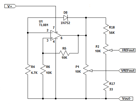
Reference Circuit Operation
Observe the Reference Circuit schematic and you'll notice that the voltages on the A and B inputs of the TL081 are easy to describe:
Va = Vo * R6 / ( R5 + R6 )
Vb = Vo - Vz where Vz is the zener diode voltage
The output voltage Vo depends on Va and Vb according to the equation:
Vo = A * (Va - Vb)
If A is very large, then Va and Vb will need to be almost exactly the same for Vo to settle at some value other than +V and -V. What we need to know is the value of Vo after the circuit powers up and Va and Vb stabilize. An easy way to do this is write the OpAmp equation expanding Va and Vb, set Vo on the left side of the equation to 0, and then solve for Vo on the right side of the equation:
Vo = A * (Va - Vb)
then
0 = A * [ ( Vo * R6 / ( R5 + R6 ) - ( Vo - Vz ) ]
Next plug in the known values for R5 (10K), R6 (10K), and Vz (5.6). For now, assume we don't know what A is:
0 = A * [ ( Vo * 10K / ( 10K + 10K ) - ( Vo - 5.6 ) ]
0 = A * ( Vo * 0.5 - Vo + 5.6 )
Last, rearrange the equation to solve for Vo:
0 = ( A * Vo * 0.5 ) - ( A * Vo ) + ( A * 5.6 )
- ( A * 5.6 ) = ( A * Vo * 0.5 ) - ( A * Vo )
- ( A * 5.6 ) = A * Vo * ( 0.5 - 1 )
- ( A * 5.6 ) / A = Vo * ( 0.5 - 1 )
- ( 5.6 ) = Vo * ( 0.5 - 1 ) notice that A ended up getting cancelled out so we didn't need to know its value
Vo = -5.6 / -0.5
Vo = 11.2V notice that the signs cancelled leaving a positive result
So for a Zener voltage of 5.6V, the OpAmp multiplies that voltage by 2 and produces an +11.2V reference voltage for Vo.
The reference voltage is then sent to the Voltage and Current potentiometers (P1, P2) that allow selection of the power supply output voltage and output current.
Questions and Answers
1. Why use an OpAmp?
The primary advantage of this circuit is that the reference output voltage Vo is virtually unaffected by the ripple voltage on C1. The output Vo of a good OpAmp is insensitive to changes in V+ or V- as long as Vo is kept somewhere in between. A Zener diode by itself, due to it's internal impedance, would be sensitive to ripple voltage on C1 which would result in a significant amount of ripple voltage on the power supply output.
2. Why use a 5.6V Zener Diode?
You'll notice on the circuit board that the zener diodes are marked as 5V1 (5.1V) but the parts supplied are actually 5V6 (5.6V). The reason the 5.1/5.6 diodes are used is due to their lower temperature coefficient which helps the power supply maintain a stable output voltage over a wide temperature range. One manufacturer may offer a better temperature coefficient on their 5.1V part while another offers the same on their 5.6V part. So I suspect (or I hope) that WeiKedz chose a part that offered better temperature stability. Attached in the PDF below are a few examples of the temperature coefficient seen from typical zener diodes.
3. Why use a reference voltage of 11.2V?
I'm now guessing as to what was on the mind of the person that designed the power supply, but based on my testing I believe the WeiKedz power supply was intended to provide 0-20V, not 0-30V as claimed. A 5.1V zener will provide a 10.2V reference while a 5.6V zener will provide a 11.2V reference. Both of these are reasonably close to 1/2 of the power supply output voltage range which helps prevent ripple voltage on C1 from affecting the reference output voltage.
4. Can I hack it?
Yes you can. Now that you know how the circuit works and what it is good for, you can use it in your own projects. To change the output voltage, simply determine the voltage you want and divide by 2, then select a zener diode with the closest voltage:
Vzener = Vo / 2
The "divide by 2" part is determined by the ratio of R5 and R6. So you can also change the output voltage by leaving the zener voltage where it is but changing R5 and R6 using the following formula:
Reference Multiplier = 1 + ( R6 / R5 )
Below are a few resistor values for different multipliers:
Multiplier x2, R5 = 10K, R6 = 10K
Multiplier x3, R5 = 10K, R6 = 20K
Multiplier x4, R5 = 10K, R6 = 30K
A precision 50K 10-Turn trimmer resistor could be used for R6 allowing the multiplier to be continuously adjusted up or down as needed instead of changing the zener diode.
Don't change the Reference voltage on the WeiKedz power supply without reading about the Error Amplifier and Current Limiter as both are designed to work with 11.2V. After you understand both of these functions, you can make the changes you want and the power supply will work as you intended.
Datasheets:
TL081 Operational Amplifier Datasheet is >>> HERE <<<
1N752 Zener Diode Datasheet is >>> HERE <<<
Temperature Coefficient Chart for Zener Diodes is >>> HERE <<<
3. Analysis - Error Amplifier Circuit
The Error Amplifier measures the power supply output voltage, compares it to the set-point voltage selected by the user, and tells the Current Pass function to raise or lower the output voltage until it matches the set-point voltage. How this is done is actually very simple but first let's take a look at a few ancillary portions of the schematic:
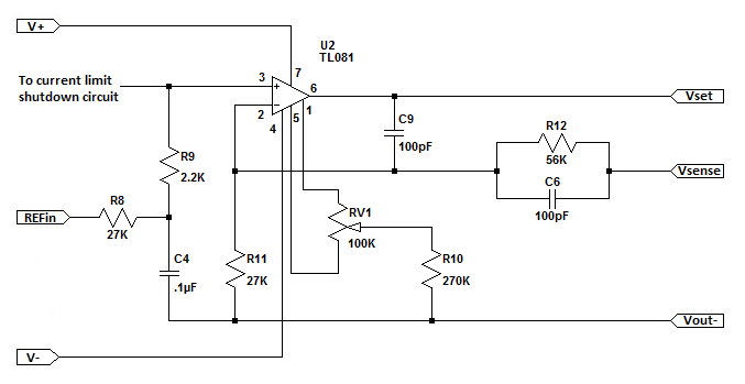
Reference Input Low Pass Filter
Notice that the set-point voltage from potentiometer P1 in the Reference Circuit passes through R8, R9, and C4 before it gets to the non-inverting input of U2. These components serve two functions:
A. Low pass filter for P1/P2
R8 and C4 form a low pass filter with cutoff frequency of:
Fc = 1 / ( 2 * pi * R * C )
Fc = 1 / ( 2 * pi * 27000 * .0000001 ) = 59 Hz
This prevents AC and RF noise pickup on the potentiometer wiring from affecting the power supply output.
B. Regulator Soft Start
To avoid power supply output ringing and possible oscillation during startup and after a current limit event, the time constant of R8 and C4 smoothly raises the output voltage over a time period of 14ms as defined by the following equation (See Illustration 1):
t = 5 * R * C
t = 5 * 27000 * .0000001 = .014 seconds
Error Amplifier Offset Null
Operational Amplifiers aren't perfect and sometimes the IC output doesn't reach the exact voltage expected due to IC variation, temperature, and external component tolerances. The difference between the expected output voltage and the actual output voltage is called the "offset voltage". Normally this voltage is very small and doesn't affect the operation of a typical OpAmp circuit. But in precision control circuits it can be critical that offset be removed or "nulled out". The TL081 provides an optional set of pins to do this. Trimmer resistor RV1 and fixed resistor R10 comprise the external null adjustment for IC U2.
The TL081 datasheet and the TI best practices (attached below) recommend using a 100K trimmer resistor attached to the offset null and Vcc- pins. For the TL081, an additional 1.5K resistor is used to avoid shorting either offset null pin to Vcc- when the trimmer resistor is rotated to the left or right extreme. What this arrangement does is balance the current mirror output in the differential amplifier section of the OpAmp IC (See section 8.2 of the TL081 datasheet).
However, the WeiKedz design does not attach the trimmer resistor to Vcc- and the tail resistor R10 is 270K instead of the recommended 1.5K. The value of R10 (270K) was likely chosen so that the offset adjustment makes full use of RV1s adjustment range. But the attachment to the power supply output ground is a mystery and may be a design error. This arrangement likely works because the Vcc- voltage is so small (-5.6V) compared to the Vcc+ voltage (+32.5V).
Current Limit Signal
The Error Amplifier input is connected to the Current Limiter output through diode D9. In the WeiKedz power supply I built, this not a over-current shutdown feature. It's actually a fold-back current limit feature that reduces the set-point voltage at the Error Amplifier until the output current falls below the current limit set-point. To completely turn off the power supply voltage output, the current limiter output must be able to go negative by at least -0.7 volts due to the voltage drop on diode D9. This is one reason the negative 5.6V power supply is needed.
And now... The Error Amplifier
I've saved the simplest (maybe) part for last. The Error Amplifier is a simple non-inverting amplifier described by the following standard equation:
Vout = Vref * ( 1 + R12 / R11 )
However, the feedback loop is not connected to the output of U4. It's connected after the Current Pass function which has a DC voltage drop of 1.4V. So the standard equation needs to be modified:
Vout = Vref * ( 1 + R12 / R11 ) + 1.4
The closed-loop DC gain of the amplifier is:
Acl = 1 + R12 / R11 = 1 + 56K / 27K = 3
The Voltage Reference circuit described in the previous step includes a set-point potentiometer P1 which provides a voltage to the Error Amplifier between 0 and 11.2V. The Error Amplifier output to the Current Pass section is therefore between:
Vout = ( Vref * Acl ) + 1.4 = ( 0 * 3 ) + 1.4 = 0V
and
Vout = ( Vref * Acl ) + 1.4= ( 11.2 * 3 ) + 1.4 = 35V
For a given reference voltage range, the Error Amplifier voltage range can be changed simply by changing the values of R11 and R12.
When the set-point reference voltage is set with P1, the error amplifier will continuously compare the power supply voltage to the set-point and and adjust its output voltage up or down so that the power supply output voltage does not change regardless of load current.
However, there are three problems with the Error Amplifier output voltage range:
A. U2 (TL081) Maximum Output Voltage Swing
The datasheet for the TL081 OpAmp specifies that the output can swing no closer than 1.5V of Vcc+ or Vcc-. The maximum output voltage on U2 when the power supply is unloaded is:
Vout = Vp - 1.5 = 32.5V - 1.5V = 31V
Remember that the Error Amplifier is connected to the Current Pass function which drops 1.4V from the Error Amplifier output. So the actual maximum voltage to a test circuit attached to the power supply is:
PSout = Vout - 1.4V = 31V - 1.4V = 29.6V
Keep in mind also that the maximum voltage swing used above is a typical value at 25 DegC. Results will vary. The minimum peak output voltage swing in the data sheet is 3V below Vcc+ which would make the power supply output voltage closer to 28V. There is not enough headroom on U2 to reliably generate a 30V output. This is not a 0-30V power supply.
B. Unregulated output when P1 is rotated to its fullest extent
If you remember from the Rectifier and Filter circuit described earlier, the peak unloaded voltage on C1 was around +32.5V and the power supply schematic shows that C1 is used for the +Vcc supply on Error Amplifier U2. Adjusting Reference potentiometer P1 to its highest range will saturate the output of U2 at 31V resulting in an unregulated 29.6V output from the power supply. The cooling fan included with the kit consumes around 100ma which will produce approximately 1Vpp of ripple out of the supply. This ripple voltage will appear at the power supply output to your circuit, which is highly undesirable.
C. Loss of regulation under load
This problem was also discussed in the Rectifier and Filter circuit. With a 1A to 3A load, the ripple voltage on C1 varies between approximately 2.5Vpp to 7.5Vpp. The power supply I built varied between 2Vpp and 6Vpp. For the Error Amplifier to stay in regulation, its output must be below the ripple voltage on C1:
Vout = Vp - Vr - 1.5V where Vp is the peak voltage in C1 and Vr is the ripple voltage on C1. The 1.5V term is the U2 saturation voltage.
Solving this equations for a variety of output currents reveals:
Vp = 32.5V, Vr = 2.5V @ 1A
Vout = 32.5V - 2.5V - 1.5V - 1.4V = 27.1V
PSout = 27.1V - 1.4V = 25.7V
Vp = 32.5V, Vr = 5V @ 2A
Vout = 32.5V - 5V - 1.5V = 26V
PSout = 26V - 1.4V = 24.6V
Vp = 32.5V, Vr = 7.5V @ 3A
Vout = 32.5V - 7.5V - 1.5V = 23.5V
PSout = 23.5V - 1.4V = 22.1V
So the maximum regulated power supply output voltage is between 22.1V and 25.7V depending on load current.
A 5.6K fixed resistor or 10K trimmer inserted above potentiometer P1 will allow the voltage set-point range to be reduced so that regulation will be maintained throughout the full rotation of P1 for all load currents. But this solution limits the power supply output voltage range to 0 - 20V. And it doesn't address the other problems discussed earlier.
Error Amplifier Feedback Frequency Response and Slew Rate Limiting
The Error Amplifier is as its name suggests, is an amplifier. It has gain. As such, if careful design steps aren't taken an amplifier can reinforce noise and harmonic frequencies generated by your test circuit or become a high frequency oscillator just sitting on the bench, which will do your test circuit and your lab not a bit of good. To prevent that, two features were added to the Error Amplifier circuit:
Feedback Low Pass Filter
The addition of C6 to feedback resistors R11 and R12 form a low pass filter with cutoff frequency approximately 32Khz.
Slew Rate Limiter
The TL081 OpAmp has a maximum slew rate of 13V/uS (13,000,000V/S !!!) which is exceptionally fast for such a simple low-cost IC. It is capable of moving from the recommended +V power rail to the -V power rail in about 2uS. The addition of C9 between the U2 output and inverting input pin limit the OpAmp slew rate to around 50uS. Without C9 the output of U2 tends to overshoot and ring with sudden changes in the power supply output voltage. C9 also ends up in parallel with C6 to drop the feedback filter cutoff frequency to 16Khz. Frequency response rolls of to unity gain around 100Khz which helps prevent the power supply from becoming an oscillator.
Datasheets:
TL081 Operational Amplifier Datasheet is >>> HERE <<<
TI Offset Null Recommendations is >>> HERE <<<
4. Analysis - Current Limit Circuit
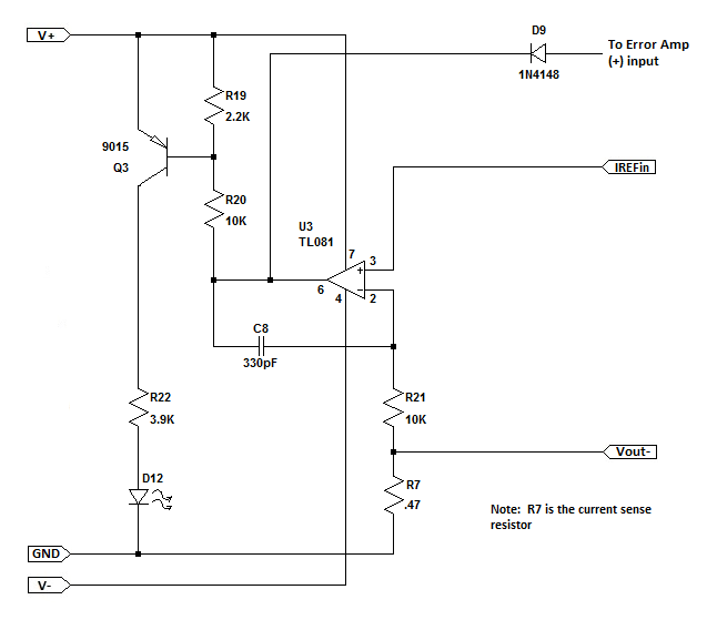
The current limiter circuit is one of the simpler function blocks. It's job is to measure the voltage on the current sense resistor and compare it to the current set-point voltage. Initially the output of the limiter is near the V+ power rail, but switches toward the V- power rail when the current set-point is exceeded. This reduces the reference voltage to the Error Amplifier and keeps the regulator output current at the current set-point.
Voltage Comparator
Remember how an ideal OpAmp works and this circuit is easy to understand. The equation for the output of U3 is:
Vo = A * (Va - Vb) where Va is the voltage on the non-inverting (+) input pin and Vb is the voltage on the inverting (-) input pin.
When there is no feedback network attached to U3, gain A is a very large number so the output of U3 can be described as follows:
Vo = 0, when (Va - Vb) = 0
Vo = V+ (V+ is the positive power supply voltage), when (Va - Vb) > 0
Vo = V- (V- is the negative power supply voltage), when (Va - Vb) < 0
This is the simple definition of a voltage comparator. In practical circuits, however, it is nearly impossible for Va and Vb to be equal so the last two equations are the ones that are important.
Current Sensing
The current sense resistor R7 is a small value power resistor (sometimes referred to as a "shunt") that works as a current-to-voltage transducer. It's value must be small so that only a minimal amount of energy is lost, but it also must be large enough to produce a measurable voltage for U3. The relationship between the current through R7 and the voltage on R7 is:
Vr = I * R where I is the power supply output current and R is the value of R7. So for various output currents the voltage on R7 is:
Vr = 0 * 0.47 = 0V when I is 0 Amps.
Vr = 1 * 0.47 = 0.47V when I is 1 Amp.
Vr = 2 * 0.47 = 0.94V when I is 2 Amps.
Vr = 3 * 0.47 = 1.41V when I is 3 Amps.
The current sense voltage can vary between 0V and 1.41V when output current varies between 0A and 3A. This is the voltage range that will be compared to the current limit set-point voltage.
You will notice that R7 is physically large. Even though the resistance of R7 is small, the current through it will be quite high and a good deal of heat will be produced. The surface area of R7 needs to be large enough for that heat to be exchanged with the surrounding air. Otherwise R7 can become so hot it self destructs. The work done (Power) in the form of heat in Watts by R7 is described as:
P = Io^2 * R7 where Io is the power supply output current
Solving this equation for the power supply maximum rated current of 3A results in:
P = 3^2 * 0.47 = 4.23W
This is dangerously close to the 5W maximum rating of R7. At 4.3 W power the resistor surface temperature will reach 117 Deg C (242 Deg F) in less than a minute. "Don't touch this" comes to mind and that heat needs to be removed if the power supply is placed in an enclosure. The WeiKedz kit provides a fan for this but you will need to remove it from the heatsink so that air can be moved across the entire power supply, not just the heat sink.
Current Limit Set-Point
Potentiometer P2 is used to provide the set-point current limit voltage. It's a simple voltage divider composed of P2, R17, and R18. The set-point voltages that can be obtained from P2 are described by:
Vccw = Vref * ( R17 / ( R17 + P2 + R18 )) where Vref is the reference voltage of 11.2V and Vccw is the voltage on U3 Pin3 when P2 is fully counter-clockwise.
Vcw = Vref * (( R17 + P2 ) / ( R17 + P2 * R18 )) where Vref is the reference voltage of 11.2V and Vcw is the voltage on U3 Pin3 when P2 is fully clockwise.
Solving these equations using the known values gives the following voltages for Vccw and Vcw:
Vccw = 11.2 * ( 33 / ( 33 + 10000 + 56000 )) = 0.0056V
Vcw = 11.2 * (( 33 + 10000 ) / ( 33 + 10000 + 56000 )) = 1.70V
Because OpAmp U3 is acting as a voltage comparator its output will shift from V+ to V- only when the current sense voltage is greater than the current set-point voltage. So the minimum and maximum power supply output currents can be calculated as:
Iccw = Vccw / R7 = 0.0056 / 0.47 = 12mA
Icw = Vcw / R7 = 1.70 / 0.47 = 3.62A
In the kit I built, I didn't want 3A of current so I changed the value of R18 to 200K which changed the output current limit range between 4mA and 1.14A. You can use the above equations to define your own ranges by changing the values of R17 and R18.
Slew Rate Limiting
As was mentioned in the previous step, the TL081 OpAmp has a maximum slew rate of 13V/uS which allows it to traverse the recommended +V/-V power rails in about 2uS. This is fast enough for parasitic inductance and capacitance to induce ringing and oscillation in the power supply. To prevent that, C8 was added to limit the slew rate from 13V/uS to around 0.3V/uS. Fast enough for the current limiter to do it's job, but not so fast that current control is lost.
Current Limit Indicator
The current limiter includes an indicator feature that lights an LED when current limiting is engaged. When U3 output falls to around 28V, PNP transistor Q3 is forward biased through resistors R19 and R20 as described in the formula:
Vo = ( V+ ) - ( VBEsat * ( R19 + R20 )) / R19 where V+ is the voltage on C1 and VBEsat is the forward biased base-emitter saturation voltage for the SS9015 PNP transistor (see data sheet below).
Solving this equation results in:
Vo = 32.5 - ( 0.82 * ( 2200 + 10000 )) / 2200 = 27.95V
When Q3 turns on, almost the full V+ voltage is applied to R22/D12. Typical maximum LED current is 20ma to 30mA with a forward voltage of 2V to 3V so it's best to check the datasheet or test the LED before deciding on the value of R22. The LED I received in the WeiKedz kit turned on at 2V forward voltage with almost 2.4V at 10mA. The designer of the kit elected to limit diode current to approximately 7.8mA which is plenty of brightness:
ILED = ( V+ - VLED ) / R22 = ( 32.5 - 2.2 ) / 3900 = 7.8mA
Power dissipated in R22 is:
P = ILED^2 * R22 = .0078^2 * 3900 = 237mW
That's very close to the 250mW rating of R22 but I'll allow it since the LED will only be turned on when the current limiter is activated. The user will then likely intervene and increase the current setting or turn off the power supply.
Datasheets:
1N4148 Diode Datasheet is >>> HERE <<<
SS9015 Transistor Datasheet is >>> HERE <<<
TL081 Operational Amplifier Datasheet is >>> HERE <<<
5. Analysis - Current Pass Circuit
The Current Pass function is the workhorse of the power supply. It's job is provide a fixed output voltage regardless of the size of the load attached to the power supply (depending on the current limit set-point or the maximum current rating of the supply).
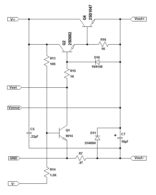
The active elements in this function block are Q2 (2SD882) and Q4 (2SD1047). These two transistors are wired in a Darlington configuration which provides an extremely high input impedance (>50K Ohms) to the Error Amplifier and a very low output impedance (<0.1 Ohms) to the load and very high DC current gain (>10,000). The Darlington configuration comes with a few disadvantages:
A. Output voltage is 1.4V lower than the input voltage due to the combined Base/Emitter junctions of Q2 and Q4.
B. Slower switching speed due to Base-Emitter capacitance of Q4.
C. Higher power dissipation in Q4 when used as a switch due to 0.7V saturation voltage limitation.
There is nothing we can do about the first limitation other than account for it in the design. To minimize the effect of B-E junction capacitance in Q4, it is common to add a resistor (R16) between the Base and Emitter terminals of Q4. This is a recommended practice but not strictly needed in a general purpose analog variable power supply. Testing of the WeiKedz power supply I built shows no change in the performance of the Current Pass function when R16 is omitted. The slew rate limiting applied to the Error Amplifier and Current Limit functions eliminate any benefit of R16. The 3rd limitation doesn't apply to an analog variable power supply.
The output voltage is described by the following equation:
Vout+ = Vset - 1.4
Notice that the Error Amplifier voltage sense input is connected to the output of the Current Pass function, so the 1.4V drop in Q2/Q4 is automatically accounted for. The error amplifier output voltage will always be 1.4V higher than the desired output voltage of the power supply.
All other components in the schematic are ancillary functions. Q2 and Q4 are doing all of the work. There is one issue with the WeiKedz design as you'll see when reviewing the datasheet for Q2 (2SD882):
When the power supply output voltage is set to 0V, the maximum Vceo rating of Q2 is exceeded by 2V (see attached 2SD882 datasheet). The transistor Base terminal is not open-circuit as specified in the rating, but exceeding Vceo under any circumstances is bad practice. Temperatures higher than 25DegC can result in the Collector-Emitter junction breaking down unexpectedly. A C-E short-circuit in Q2 will cause the power supply output to suddenly change to V+ (32.5V) with current limiting disabled, potentially destroying the circuit attached to the power supply. This is further evidence that the WeiKedz power supply was not designed for 0-30V as specified.
-5V Failure Shutdown
The -5V supply is required for the variable power supply to operate properly. Without it, the Error Amplifier and Current Limit functions become unstable. R13, R14, and Q1 form a shutdown circuit for the Current Pass function if the -5V power supply falls below approximately -3.8V. Q1 will be saturated by R13 shorting the output of Error Amplifier U2 to ground, which turns off Q2 and Q4 and drops the power supply output to 0 volts. U2 is internally protected from short circuit to ground or to either of the power supply pins.
However the maximum U2 IC dissipation (650mW at 25DegC) cannot be exceeded during an output short circuit event. This is not a problem when operating the TL081 at the recommended +/- 15V power supply voltages. Short-circuit output current for the TL081 is internally limited at 20mA. But when using a +32.5V supply and adding in the TL081 operating current of 1.4mA, shorting U2 output to ground will result in 700mW of device dissipation. This is a bad thing if the -5V supply fails and the operator doesn't notice. U2 will likely overheat and self destruct. During testing of the power supply I built, lifting R14 from the PCB overheated U2 in less than a minute. Using a 20VAC transformer instead of a 24VAC transformer reduced U2 dissipation to 500mW which is still high but manageable. Yet one more data point that makes me believe this power supply circuit was not intended for a 30V output.
C7 Discharge
C7 is included to improve output voltage stability when powering circuits with small but rapid changes in load current. However, C7 doesn't have a low impedance discharge path if no load (or very light load) is attached to the power supply. The only path available is the large value resistors R11/R12 (83K Total) in the Error Amplifier. If the power supply output voltage is set to maximum, and then quickly set to zero, Q4 Base-Emitter junction will be reverse biased and no current will flow through the Current Pass function. It will then take over 4 seconds for C7 to discharge through R11/R12 according to the following:
Discharge Time = R * C * 5 = ( 56000 + 27000 ) * .00001 * 5 = 4.15 seconds
This will be visible if a volt meter is used to measure the power supply output, and can make adjusting the power supply difficult without a load attached.
To prevent this, D10 and R15 were included to provide a low impedance discharge path for C7. If the reference voltage falls below the output voltage, D10 will be forward biased which results in R15 being connected across C7. The discharge rate for C7 will then be:
Discharge Time = R * C * 5 = 1000 * .00001 * 5 = .05 seconds
R11/R12 were not included in the above equation because their combined value is so large that R15 dominates.
Reverse Output Voltage Protection
To protect the power supply from reverse voltages attached to the output (charged capacitors, batteries, another power supply, etc.) diode D11 is attached across C7. If a voltage greater than -0.7 volts is attached to the power supply output, D11 will conduct preventing the voltage from rising further until the offending voltage is removed or D11 is destroyed.
Datasheets:
1N4004 Rectifier Diode Datasheet is >>> HERE <<<
1N4148 Diode Datasheet is >>> HERE <<<
2SD882 Transistor Datasheet >>> HERE <<<
2SD1047 Transistor Datasheet >>> HERE <<<
SS9014 Transistor Datasheet >>> HERE <<<
6. Assembly Manual for Transformer Operation
I've re-written the assembly manual for the WeiKedz Variable Power Supply to make it easier to follow and included some part placement and soldering tips for those wanting the benefit of better illustrations before attempting an this electronics project.
I've also included an Operation and Maintenance guide for use after the project is assembled. This guide will provide some assistance and suggestions for attaching a transformer to the power supply, and also includes detailed description of each power supply function block.
Assembly Manual is >>> HERE <<<
Component Identifier is >> HERE <<
Operation and Maintenance Manual is >>> HERE <<<
This concludes Part 1 of the Portable Variable Power Supply article which hopefully has given you a solid understanding of how the Weikedz power supply works. Next, I'll describe how to put the information to use modifying the power supply from transformer to battery operation, and how to add a V/I meter to make a more useful portable variable power supply.
Ultrasonic Range Finder
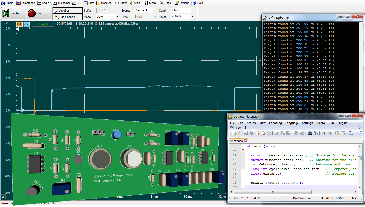
When I started my career in control systems I was fascinated with the many different ways that machines could be interfaced to the environment they operated in. Limit switches (electrical and optical), encoders, resolvers, strain gauges, thermocouples... the control system engineer had a long list of sensors to choose from. And the list has grown even longer following successful innovations in micro machining. Today the sensor and conditioning electronics, and even a microprocessor for signal processing, are integrated on a chip. Sensor integration has helped make machine control systems smaller and easily distributed throughout a given process. But they have also obscured what actually goes on inside the black box. As a design engineer, I enjoyed reading schematics and taking sensors apart to figure out how they did what they did. I learned quite a bit about how noisy and stressful the outside world is on sensitive electronics, and how challenging it can be to reliably separate out a desired signal from industrial background noise.
At first glance, the theory behind an ultrasound range finder seemed intuitive and there were a number of small and inexpensive ultrasound sensors available commercially. But all of these are highly integrated mixed-signal products that would have been difficult to fully understand and experiment with using an oscilloscope and pulse generator. So I decided to design my own and see how ultrasonic waves propagate, reflect, and interfere in a given space. My goal was to design a circuit that could reliably detect an object 1 to 10 feet from the sensor using digital control signals from a small computer like a Raspberry Pi or Arduino. The analog ultrasound range finder would generate the carrier pulse and detect the carrier reflection. The computer would control transmitter timing and convert the carrier reflection time delay into a distance.
This project was a fun exercise in simple analog design with digital interfacing and software programming. For those interested in giving a project like this a try I've included a very detailed assembly manual, lots of pictures, theory of operation, parts list, software, and complete schematics.
Obtain The Assembly Manual

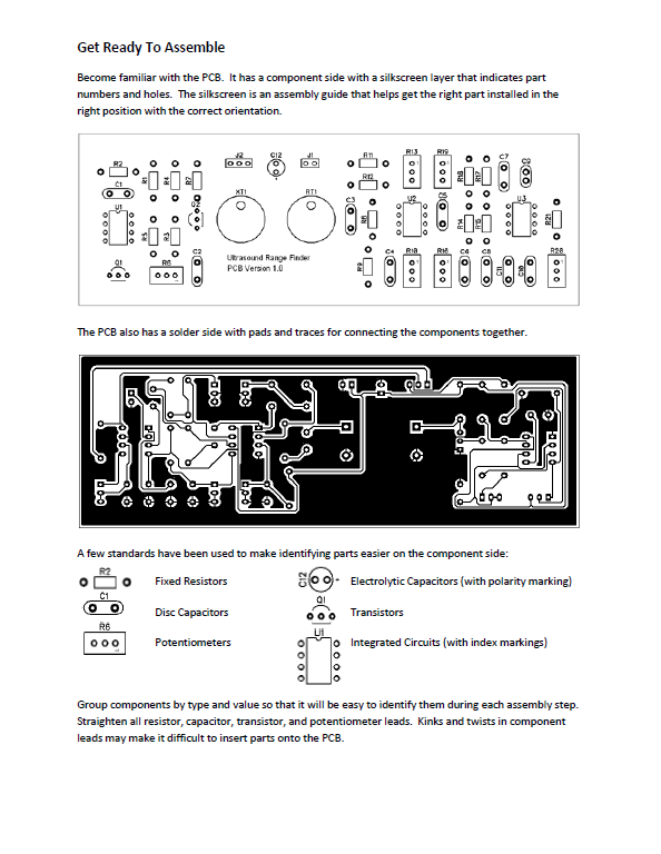
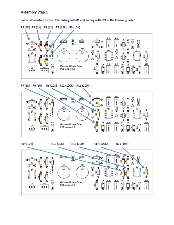
The Analog Ultrasound Range Finder project in this article was constructed by following the steps in the Assembly Manual found >>> HERE <<<. The assembly manual contains the following useful information:
1. Basic soldering and assembly techniques.
2. Step-By-Step illustrated assembly instructions.
3. Testing and Alignment Procedure.
4. Troubleshooting Procedure.
5. Parts List.
6. Circuit Schematics
The PCB layout for the range finder project was made using the free version of Diptrace (www.diptrace.com) which works really well for small projects on double-sided or single-sided boards. The Diptrace schematic files, PCB layout files, and PCB toner templates can be obtained at the links below:
For single run prototype PCB projects I use the toner transfer process and materials from Pulsar Professional FX's product "PC Fab-In-A-Box" (www.pcbfx.com). Their process has worked well for me. I run the toner prints with an HP Laserjet P2035 with toner density turned full up. I do the transfers with an Apache AL13P which can do boards up to size A at 390 DegF. After that I sponge on some warmed up Ferric Chloride for a few minutes until unwanted copper is removed. The PCBFX products work really well for the work I do and can reliably lay down some really fine lines.
NOTE: As of 2026, Pulsar Professional is no longer in business. I have left the content here for historical purposes.
Obtain Components Listed in the Assembly Manual Parts List
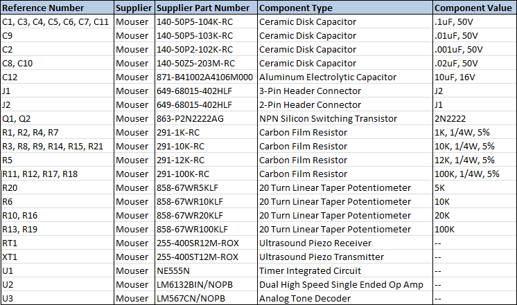
Review the parts list and obtain the components indicated. Below are a few notes regarding the parts used for the Analog Ultrasound Range Finder:
1. I purchased all of the parts from Mouser (www.mouser.com) but you can obtain them from Digikey, Sparkfun, or another distributor. If you use another source, be sure to review the datasheets to make certain the parts have the same physical dimensions and lead spacing as the ones I've specified or they may not fit on the PCB.
2. 20-Turn trimmer resistors are highly recommended as amplifier and oscillator parameters require fine adjustment.
Please Note: I have no business relationship with any of the above vendors. Nothing of financial value was exchanged for my recommendation. None of the above vendors provided compensation of any kind during the creation of this project. I will not be compensated in any way if you choose to build this project or purchase components from any vendor I recommend. I simply had a good experience with the vendors I recommend and believe you will too.
Review the Schematic to Become Familiar With the Range Finder Transmitter Design
Transmitter Design
The Ultrasound Transmitter is a simple 555 astable oscillator circuit with a frequency of 40KHz and a duty cycle near 50% (i.e. square wave output). I used the circuit topology recommended in the datasheet for an astable oscillator. No sense "reinventing the wheel" when a perfectly good circuit is provided by the manufacturer.
The oscillator is switched on and off via common collector Q1 which is connected to the 555 reset pin. An active high on the base of Q1 brings the 555 timer chip out of reset and oscillation starts. A low voltage on Q1 pulls down the 555 reset pin through R2 and oscillation stops. Q1 isolates control logic from the 555 timer reset current and ensures the reset voltage will fall below the nominal 500mV indicated in the data sheet as the TE pin falls below 1V. The 555 oscillator does not require the Control Voltage pin (Pin 5) so it is bypassed to ground via C1 as recommended in the data sheet.
According to the 555 IC datasheet, two formulas determine the oscillation frequency and the duty cycle of the transmitter output:
Frequency = 1 / (0.693 * (R4 + 2 * (R5 + R6)) * C2)
Duty Cycle = (R5 + R6) / (R4 + 2 * (R5 + R6))
The duty cycle equation indicates that for a near 50% output on/off ratio, the value of of R4 should be very low compared to the combined value of R5 and R6. However, because the Discharge pin will go low to discharge C2 the value of R4 cannot be so low as to cause the 555 IC to exceed its maximum power dissipation. The datasheet provides some guidance on the recommended Discharge pin saturation current (between 4.5mA and 15mA). A discharge saturation current of 5mA was chosen so that a common 1K resistor could be used for R4 (i.e. 5V/5mA = 1K Ohms).
In this circuit configuration the most that the Duty Cycle can practically be is around 49%, so that value is used as a starting point for determining the value of R5 and R6.
Rearranging the Duty Cycle equation to solve for the combination of R5 and R6 results in:
R5 + R6 = R4 / ((1 / DutyCycle) - 2)
Notice in the above equation that the denominator results in a singularity at 50% duty cycle.
Substitute the known values: Duty Cycle = 0.49, R4 = 1000 Ohms
R5 + R6 = 1000 / ((1 / 0.49) - 2) = 24,500 Ohms
Now to check if the above resistance can be used with a standard capacitor value.
Rearranging the Frequency equation to solve for C2 results in:
C2 = 1 / (F * 1.386 * (R5 + R6))
Substitute the known values: F = 40,000 Hz, R5 + R6 = 24,500 Ohms
C2 = 1 / (40000 * 1.386 * 24500) = 736pF
I prefer to use the most common disk capacitor values in order to avoid potentially high costs and supply issues, so for this design I rounded up to .001uF (aka 1000pF).
Now that a suitable value has been chosen for C2, rearranging the Frequency equation to adjust the value of R5 + R6 results in:
R5 + R6 = 1 / (F * 1.386 * C2)
Substitute the known values: F = 40,000 KHz, C2 = .000000001 Farads
R5 + R6 = 1 / (40000 * 1.386 * .000000001) = 18,038 Ohms
I typically try to choose a combination of values for R5 and R6 so that the target frequency is obtained when R6 is adjusted near it's midpoint. This allows plenty of room for adjusting the oscillator frequency up or down as needed. So I chose a 12K Ohm resistor for R5 and a 10K trimmer for R6. By adjusting R6 to around 6K Ohms, the desired 18K Ohms is achieved with plenty of room to adjust for a near exact 40KHz.
Now that suitable values for R5, R6, and C2 have been chosen, the standard Duty Cycle equation can be used to verify the desired duty cycle is near 50%:
Duty Cycle = (12000 Ohms + 6000 Ohms) / (1000 Ohms + 2 * (12000 Ohms + 6000 Ohms)) = 48.6%
Almost perfect! The last step is to add a driver to the 555 IC output.
The 555 IC datasheet indicates that the Output pin (Pin 3) can source and sink 200mA of current, but not at the rated Vcc applied to the chip. In order to obtain the highest voltage swing possible across transmitter XT1, I used a common emitter Q2 in parallel. When the 555 IC output is low, XT1 is driven close to Vcc through R7. When the 555 IC output is high, Q2 shunts XT1 driving it's voltage to near zero. R7 limits the Vcc shunt current through Q2 to 5mA while protecting XT1 from excessive charge current. R3 was chosen to ensure that Q2 fully saturates when the 555 IC Output pin goes high. Transmitter XT1 behaves like a parallel LC resonant circuit tuned to 40KHz with Q of around 40. Therefore, Q2 serves another important purpose: Damping XT1 so that the ultrasound output cuts off within 1ms after the 555 IC is disabled.
Review the Schematic to Become Familiar With the Range Finder Receiver Design
The receiver design is significantly more complicated than the transmitter design. There are several circuit adjustments provided so that the amplifiers can be reconfigured for different types of receivers (time delay, doppler, interferance, etc). I will cover only the Time Delay receiver type in this article in order to keep it as short as practical.
Simple Sonar Example
The "Simple Sonar" example above describes what the transmitter and receiver are trying to do. An ultrasound wavefront propagates from the transmitter, bounces off of a target, and is detected by the receiver. By measuring the round trip time between the start of transmission and the detected reflection, and comparing that to the propagation velocity of sound, the distance between transmitter and target can be calculated. The formula is:
Distance = (Round Trip Time / 2 ) * Velocity of Propagation
In the real world, however, the problem is much more complicated as illustrated in the "Complex Sonar" example below. I won't force you through a rigorous explanation of the receiver design math but below are just a few of the parameters that have to be considered:
1. Ultrasound Transmitter Minimum Power and Dispersion Angle
2. Ultrasound Receiver Sensitivity
3. Minimum detector signal threshold
4. Target Reflection Coefficient
5. Distance, Air Density, and Air Flow effects on Sound Attenuation
6. Temperature, Humidity, and Elevation effects on Propagation Velocity
7. Time delay and signal strength effects of multi-path interference
A Real-World Sonar Example
The receiver presented in this article was designed to detect a large, unobstructed, stationary target at a maximum distance of 10 feet, and smaller targets at a maximum distance of 6 feet. The actual distances that can be measured depend on how large the target is, how reflective the target is, how quickly the target is moving, how many obstacles exist between the sensor and the target, and to a lesser extent how active the air is between the sensor and the target.
The ultrasonic transducers used (RT1 and XT1) are piezoelectric devices that are optimized to ether change shape when a voltage is applied (transmitter transducer) or produce a voltage when struck by ultrasonic sound waves (receiver transducer). Both devices use quartz crystals that exhibit reactive properties when energized by an AC signal source. The equivalent circuit for each is a parallel resonant RLC circuit with 2400pF capacitance, 6.6mH inductance, and 1600 Ohms resistance. The receiver transducer has an area of less than 1cm^2 and a sensitivity of 398uV per ubar of sound pressure. We will need an amplifier with input impedance at least 5X the transducer impedance to capture as much of the signal voltage as possible, and the amplifier will need very high gain so that the small transducer voltages can be magnified enough to do something useful.
1. The receiver circuit is intended for a single supply voltage of +5V. So a good Op-Amp for this design is one optimized for a Single Ended Supply (+2.5V to +24V) and Rail-to-Rail Output (+0.1V to +4.99V).
2. The receiver circuit must provide high gain at high signal frequency. So a good Op-Amp for this design needs a high gain bandwidth product, and a high slew rate.
Slew Rate in Volts/uS = 2 * pi * Frequency * Vp * .000001
Gain Bandwidth Product = Frequency * Gain
Substituting the known circuit parameters: Frequency = 40,000 Hz, Vpp = 5V, Max Gain per Stage = 100
Slew Rate = 2 * pi * 40000 * 5 * .000001 = 1.26V/uS
Gain Bandwidth Product = 40000 * 100 = 4,000,000 Hz or 4MHz
3. The amplifiers are standard inverting designs that will operate on a regulated supply, so Power Supply Rejection and Common Mode Rejection aren't critical and can be around 80db which is typical for many Op-Amps.
4. There are two gain stages in this design and the PCB needs to be reasonably small, so a dual Op-Amp in an 8-pin package would be best.
As an analog designer I'm somewhat partial to TI products so entering the target parameters above into their product website shortened the list down to 6 candidates. One Op-Amp stood out as an excellent choice with respect to features and cost:
TI LM6132 Dual Low Power 10 MHz Rail-to-Rail Operational Amplifier
The specifications for this chip exceeded the needed parameters. The trade-off is that the LM6132 can only drive high impedance loads (10K is recommended). But in every other respect, it's a good choice.
Receiver Design - Carrier Amplifier and Carrier Limiter
The LM6132 is operated with a single +5V power supply, so the amplifier needs an input DC bias voltage to set the output to the desired DC offset voltage. Adjustable voltage dividers R9/R10 and R15/R16 provide the bias voltage to the non-inverting input (pins 3 and 5) of each Op-Amp. Increasing the bias voltage to the non-inverting input increases the output offset voltage. Decreasing the bias voltage to the non-inverting input decreases the output offset voltage. Capacitors C4 and C6 prevent high frequency power supply noise from affecting the Op-Amp output.
The LM6132 data sheet recommends a load resistance of 10K to achieve the output swing and slew rate specifications, so a 10K input impedance was chosen for both amplifiers via R8 and R14. This also meets the design goal of an input impedance roughly 5X the receiver transducer impedance discussed earlier. The standard formula for an Op-Amp inverting amplifier gain (A) is:
A = - Rf / Rin where Rf is the feedback resistor and Rin is the input resistor.
However for a maximum stage gain of 100, the Rf value would need to be 1Meg Ohm. I prefer not to use resistors over 100K in feedback circuits and especially not 1Meg trimmer resistors. They are extremely noisy and difficult to adjust. So instead, for amplifiers with large gains I recommend the modified tee feedback configuration illustrated in the receiver schematic. This feedback circuit is quieter than the simpler 1Meg trimmer design and is easier to adjust. The gain formula using the first stage as the example is:
A = R11/R8 * (2 + R11/R13)
When trimmer resistor R13 is adjusted to 33K Ohms, the Op-Amp gain is set at 50. Resistors R17, R18, and trimmer resistor R19 set the second stage gain the same way.
Receiver Design - Carrier Detector
In order to separate the transmitted carrier signal from external and internal noise, a Phase-Locked-Loop tone decoder IC (TI LM567) is used for the Carrier Detector. The detector output is an active low digital Carrier Detect (CD) signal that is easily interfaced to a micro-controller. The LM567 datasheet indicates that the input impedance in Pin 3 is 40K Ohms, which is more than high enough to keep the LM6132 Limiter output in spec. As recommended in the LM567 datasheet, capacitor C7 decouples the DC output of the Limiter from input Pin 3 and capacitor C11 helps insure a noise free power supply at Pin 4. The PLL oscillator frequency is defined by the following equation:
F = 1 / (1.1 * R * C)
Note: Manufacturers differ on the equation above so be sure to check the datasheet for the part you have!
There are many different values that can be used for R and C. I had a bunch of .02uF disk capacitors in inventory so I decided to use one of them. Rearranging the Frequency equation to solve for R when C is known results in:
R = 1 / (1.1 * F * C)
Substitute the known values: F = 40000 Hz, C = .00000002 F
R = 1 / (1.1 * 40000 * .000000002) = 1136 Ohms
So for the LM567 PLL oscillator, C10 is a .02uF capacitor and R20 is a 5K Ohm trimmer adjusted to 1136 Ohms.
For accuracy at close range, the Carrier Detector needs to lock onto the reflected ultrasound pulse in the fewest number of cycles. The LM567 datasheet indicates that the loop bandwidth and output filter play a role in the responsiveness of the detector output. Referring to the graphs in the datasheet, setting the value for C9 at .01uF allows the LM567 to lock onto the ultrasound pulse within 20 cycles (500uS) but sets the loop filter bandwidth at 14% (which is higher than desired but an acceptable trade). The datasheet recommends that the value of C8 be twice the value of C9 so a value of .02uF was chosen for C8. The LM567 output Pin 8 is an active low open collector transistor that requires an external pull-up resistor. A 10K Ohm pull-up resistor R21 has been included for convenience but the internal pull-up feature on the Raspberry Pi or Arduino I/O can be used instead.
Receiver Design - More about the Carrier Limiter
Notice that the second amplifier stage is referred to as an Amplifying Limiter. This circuit is nearly identical to the Carrier Amplifier with one exception: The input bias voltage is adjusted so that the output offset is 0V when no signal is detected. The reason for this has to do with environmental ultrasonic noise causing false triggering of the Carrier Detector. Many sources of audible noise (snapping your fingers, boiling water, metal shaping, etc.) create weak sound in the ultrasonic spectrum. This noise can cause the LM567 to generate short bursts of activity even when the transmitter isn't turned on. With careful adjustment of the Limiter, background noise can be removed from the Detector input so that the Detector output only triggers when ultrasonic measurements are being made.
Fabricate the PCB for the Range Finder

NOTE: As of 2026, Pulsar Professional is no longer in business. I have left the content here for historical purposes.
I fabricated the PCB for this article using the PCB Fab-In-A-Box starter kit from Pulsar Professional FX at www.pcbfx.com. The company offers a Starter Kit that includes the bare PCB that I used for the Range Finder board, a bunch of toner transfer paper, several toner sealing and color transfer sheets for the component silkscreen, and very detailed instructions on how to make a good PCB.
You need a decent laser printer or copier to make the transfer artwork, and a pouch laminator to transfer the toner to the PCB. I chose a refurbished HP LaserJet P2035 for the printer and an older Apache AL-13P for heat transfer. Pulsar Professional FX sells a better laminator for the same price advertised on Amazon so it's easy to order the supplies and laminator at the same time from the same place. The company is constantly testing new printer/copiers and laminators to make sure that the customer can obtain high quality results without having to spend a lot of money.
I've done three projects so far using the Starter Kit and am very happy with the results. In the past I've tried several different paper, toner, and iron transfer methods posted around the web and all of them were way more effort than the results could justify. At one point I was driving around to (the former) OfficeMax, Best Buy, Office Depot, and Staples unsuccessfully trying to find just a certain type of paper that folks were saying worked well. I gave up the method after having to wait an hour for the paper to loosen, then carefully scraping the paper off for 15 minutes, and STILL having to fill in voids and broken traces with a sharpie. Pulsar fixed the effort and accuracy problem by developing a transfer paper that holds the toner firmly during printing but releases it almost instantly in water. No soaking and scrubbing required. My last PCB took less than 15 minutes to print, trim, transfer, and etch. I've already broken even on my DIY equipment and supply costs compared to sending my projects out to a fabrication house and having to wait a week. For quick-turn home and prototype projects, PCB Fab-In-A-Box is the only way to go.
Below are the steps I followed to make the PCB:
1. Print the top component silkscreen and board outline artwork on a plain piece of paper and measure the board outline to make sure the dimensions are accurate. Some printers do not print to scale and you may have to change the print scale in your PCB application to get the correct size on paper.
2. Cut out a piece of 1/4" foam board the same size as the board outline.
3. Tape the properly scaled top component silkscreen artwork to the foam board.
4. Using the tip of a sharp pencil or a small push drill, make small holes through the foam board where the component leads go.
5. Test fit each component to make sure all the parts will fit on the PCB as marked. Make any outline adjustments in the PCB software until all parts fit.
6. If everything fits, take one sheet of paper from the printer and write "Side A" on one side and "Side B" on the other. Load the marked sheet of paper into the printer with the "Side A" mark facing up and then print the bottom trace artwork.
7. Observe which side of the paper the trace artwork was printed on (Side A or Side B). If the trace artwork printed on Side A, remember to load the printer with PCBFX toner transfer paper glossy side up. If the trace artwork printed on Side B, remember to load the printer with PCBFX toner transfer paper glossy side down.
Note: I usually load the printer with two sheets of PCBFX toner transfer paper. I print multiple copies of the trace side artwork on one sheet, and multiple copies of the component side silkscreen on the other sheet. That way if I make a mistake applying the artwork to the PCB, I can always cut out another copy and try again.
8. Turn on the laminator and set the temperature according to the PCBFX instruction sheet.
9. Fill a sink or other container large enough to hold the PCB with cold water.
10. Cut the blank PCB so that it is at least 1/8" larger than the board outline. Many times the PCB edges will be raised slightly after cutting which can interfere with toner transfer. The extra space helps ensure that heat and pressure are evenly applied to traces at the edge of the board.
11. Carefully clean the blank PCB copper surfaces to remove any slight tarnish or oil. The cleaning process should leave a slight haze on the copper that will help the toner to grip the board. Deep scratches or excessive hazing are bad so don't go overboard on the cleaning process. I clean the PCB first with liquid dish washing detergent and a polishing cloth, and then follow up with alcohol and a lint free cloth.
12. Load the PCBFX toner transfer paper into the printer using care to only touch the corners or edges where artwork will not be printed.
13. Print the artwork with the toner density setting as high as possible to achieve a dark opaque print. Be sure to use the "mirror image" setting on your PCB software so that when the transfer paper is applied the traces and text are applied correctly.
14. Trim the artwork closely to the board outline on the long edges but leave at least one to two inches on one of the short edges. Use care not to touch the applied toner with tools or fingers while trimming.
15. Place the artwork face down and centered on the clean and dry copper side of the PCB. Fold over the extra length of paper and carefully insert the PCB into the laminator folded edge first.
Note: I repeat the lamination step a few times to make sure the toner has completely fused to the copper. You may not need to do that with the newer laminators supported by Pulsar Professional FX.
16. Immediately after laminating the board, submerge it under cold water. The paper will almost immediately darken and begin to separate from the fused artwork. Wait at least 30 seconds and gently slide the paper away from the board.
17. Carefully rinse the board and pat dry with a soft cloth. Let the board fully dry before proceeding to the next step.
Note: PCBFX recommends a second lamination step to seal the toner and fill in any tiny voids that might leave holes during etching. I've tried the process with and without the sealing step and saw distinct improvement in the quality of the PCB when the sealing step is used. Especially with large dark areas prone to tiny pinhole voids and very thin traces.
18. Cut a piece of the green sealing strip to the same size as the PCB but leaving one to two inches on one of the short sides to be folded over during laminating.
19. Place the green sealing strip over the toner, fold the excess over, and feed the PCB into the laminator using slight finger pressure on the sealing strip to keep it feeding straight.
Note: I usually run the board through the laminator a few times to make sure the sealer is completely applied. You may not need to do that with the newer laminators supported by Pulsar Professional FX.
20. Peal the sealing strip from the PCB. The board is now ready for etching.
I've found that it's not necessary to use a whole tank of chemicals to etch a board. I set my PCB software to fill in empty areas of the PCB with copper which reduces the amount of chemical required and the amount of time needed, both of which help improve the quality of the etching. I use two containers: One large enough for the board, and the other large enough to hold the first container and an inch or so of hot water. I heat up some water to near boiling and pour it in the large container. Then I pour just enough chemical into the small container to cover the board, set it in the large container, and let the chemical warm up. After that I use a disposable sponge brush to gently brush the chemical onto the board until etching is complete. I can etch a board in about 5 minutes using about two ounces of Ferric Chloride.
Below are some photos of the board after etching and after the component silkscreen layer artwork was applied and holes drilled. It only took me about 45 minutes to do everything I wanted to do including drill the holes. And I really liked the way the board looked when I was done so the effort was worthwhile. The boards made with PCBFX are the best I've done outside of a professional fabrication studio and I'm using it for all of my DIY projects.
The completed Analog Ultrasound Range Finder is shown below.
Please Note: I have no business relationship with PCBFX. Nothing of financial value was exchanged for my recommendation. PCBFX provided no compensation of any kind during the creation of this project. I will not be compensated in any way if you choose to build this project or purchase supplies from PCBFX. I simply had a good experience with PCBFX and believe you will too.
Follow the Steps in the Assembly Manual to Build and Test the Range Finder
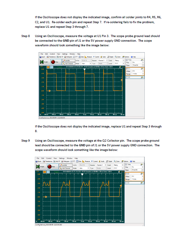
The assembly manual contains four sections of interest to the builder:
1. Basic assembly hints - Useful hints for the new builder.
2. Detailed assembly instructions - Shows what parts go where at each step in the process.
3. Test and Alignment procedure - Verifying the assembly and getting it ready for work.
4. Troubleshooting procedure - Just in case something goes wrong.
After the PCB has been fabricated, follow the steps in the assembly manual to build the Ultrasound Range Finder. The troubleshooting section will help you find and fix anything isn't working correctly.
After the range finder has been assembled and tested, an oscilloscope can be attached to the Transmitter Enable (TE) and Carrier Detect (CD) output to view the receiver and transmitter in action. The oscilloscope trace below shows the TE pin in red enabling the 40KHz oscillator. The blue trace shows the output of the PLL detector. Notice that because the receiver is so close to the transmitter when TE is enabled that the CD output goes low while transmitting and then inactive after transmission stops. A short time later, the CD pin goes low again indicating a reflection has been detected. A microprocessor will be used to measure the time delay and convert it to a distance.
The second scope trace shows the raw limiter output to the Carrier Detector in green with the CD signal in blue. The Carrier Detector does indeed change state after receiving at least 20 cycles of 40KHz carrier.
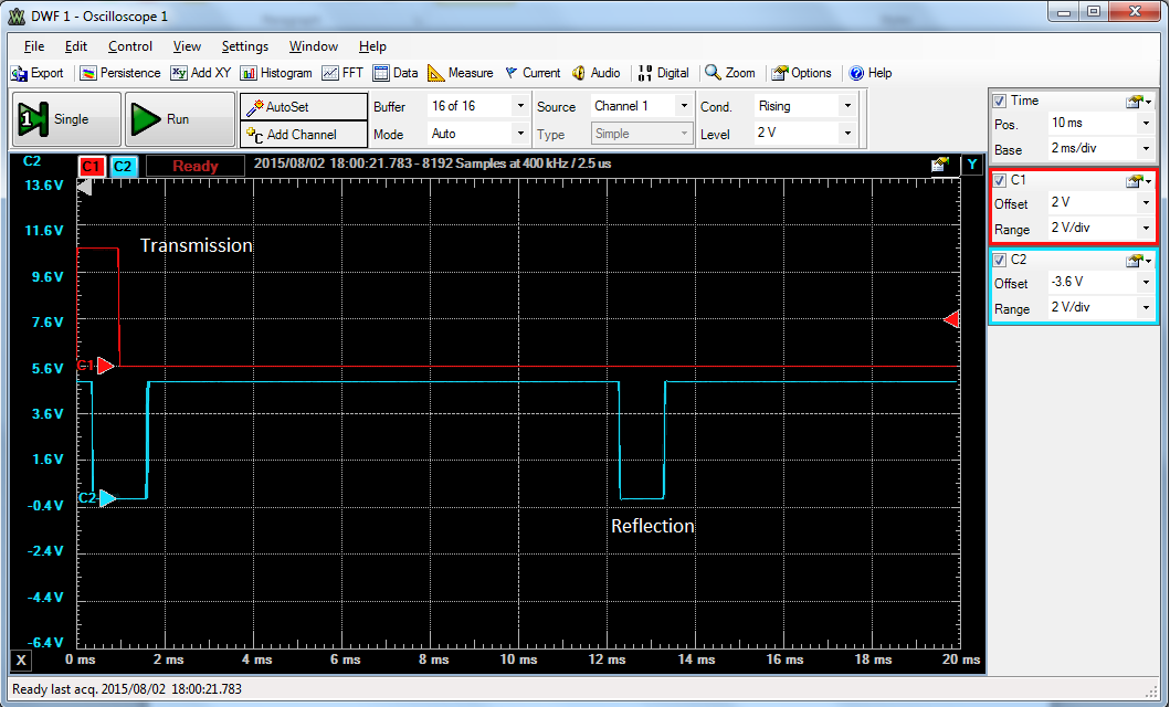
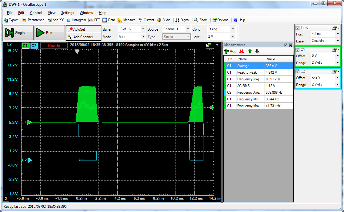
Attach the Range Finder to the Micro-controller of Your Choice
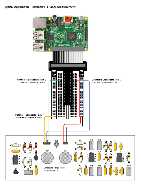
A datasheet for the Analog Ultrasound Range Finder can be found HERE.
The datasheet is a quick reference for the operating parameters of the range finder board and contains some examples for interfacing to the Raspberry Pi and TI MSP430. I did not have an Arduino board on hand to test with prior to writing this article so I won't cover it here to avoid misleading folks that want to use it. Those familiar with the Arduino family of micro controllers will readily understand how to use the simple range finder interface.
Compile and Run the Example Software
I've created a sample C program for exercising the functionality of the Ultrasound Range Finder which can be downloaded HERE.
The sonar application works in similar fashion to the IP PING utility. It generates a 1ms pulse of 40KHz ultrasound and then waits to receive an ultrasound reflection. If a target reflection is found, the target distance is automatically calculated and displayed in cm and feet. Targets are "pinged" every second until the user presses Ctrl-C.
The sonar application was compiled and tested on the Raspberry Pi 2 running Raspbian 1.4.1 and makes use of the excellent WiringPi library from Gordon Henderson which can be found at his website. The WiringPi library contains function calls similar to those found on the Arduino so it is possible to rearrange the example program to run on the Arduino platform.
The steps below describe how to build the sonar application:
1. If the WiringPi library is not already installed on your Raspberry Pi, follow the library install instructions here.
2. Download the sonar.c source file and copy it to a directory on the Raspberry Pi.
3. Build the sonar executable by entering the following command:
gcc sonar.c -o sonar -lwiringPi
4. Execute the sonar application by entering the following command:
sudo ./sonar
The sonar application will display a "Target Found..." message every second or a "Timeout" message every 2 seconds depending on whether or not an ultrasound reflection was detected.
It's possible to add multi-target detection, a UI with a bar graph showing where targets ahead are located, a display with target distance changes over time, and much more. I've left these to the reader to implement.
3 Transistor Short Wave Radio
Radio Shack advertised it's first perfboard electronics kits in 1967 and expanded the line in 1968 and 1969. By 1970 there were 26 kits available that included all the parts needed (except the battery) enclosed in a "space age pbox" that served as the packaging and the perforated board that the kit would be assembled on. The 3 Transistor Short Wave Radio project described here is based on the Radio Shack pbox kit of the same name, but it has been updated with silicon transistors and passive components and controls that can be obtained from electronics suppliers on Amazon. When I was a kid I was able to purchase the original 3 Transistor Short Wave Radio kit from the bargain bin of my local Radio Shack long after they were discontinued. I've built the updated radio kit described in this article and believe it works just as well as I remember the original kit did back in the 80's. To make it easy to replicate my work, I've provided illustrations and step-by-step assembly documentation based on the original assembly manual from Radio Shack. I do not make this kit available for sale and I've kept the original branding and copyright notices intact. What I've made available here is strictly for fun and educational purposes. I hope you have as much fun with this project as I did. The original branding, design and documentation are property of Radio Shack.
A little radio theory
If you would like to start building the radio you can skip this section. But if you are interested in knowing how this radio works then by all means, read on!
There are three major receiver types you can build with analog components:
- Tuned Radio Frequency (TRF) receiver
- Regenerative receiver
- Superheterodyne receiver
The simplest radio is the TRF receiver which can usually be constructed with only five components and requires no batteries or AC power. A TRF radio is the easiest to build but it is not very sensitive to weak signals and has difficulty distinguishing radio stations broadcasting on channels that are close together. A good antenna and ground connection is required to receive anything other than nearby high-power radio stations. A "crystal radio" is the most common TRF radio that experimenters will build.
The Regenerative receiver uses some of the same components as the TRF receiver but adds transistors to amplify the radio frequency and audio frequency signals used by the radio station. The Renerative receiver is extremely sensitive to weak signals but it is more complicated than a TRF receiver. It requires battery or AC power to operate, works best with a good antenna and ground connection, and uses two adjustments for tuning in the desired station. The 3 Transistor Short Wave Radio illustrated in this article is a regenerative receiver design.
The Superheterodyne receiver uses many of the same components as the TRF and Regenerative receivers but adds special oscillator and amplifier circuits that make tuning into the desired station very easy. This is the type of receiver upon which all modern AM/FM radios are based. The Superheterodyne receiver is sensitive to weak signals and easily distinguishes between stations that are close together. Unfortunately the superheterodyne is the most complicated of the three receiver types and thus the most difficult to build.
In order for a radio receiver to be useful it needs a transmitter within range that is broadcasting information which can be detected and converted into some useful form of energy (electrical or mechanical). A radio transmitter uses electromagnetic waves to transport information through the ground, the atmosphere, or even across the vacuum of outer space. The properties used to describe these electromagnetic waves include amplitude, frequency, polarization, and direction of propagation. The most important properties for the radios described in this article are amplitude (sometimes referred to as signal strength) and frequency (sometimes referred to as a "channel"). Because electromagnetic waves get weaker with distance, amplitude at the transmitting antenna determines how far away the receiver can be and still detect the information in the broadcast. There are many different frequencies that a radio transmitter or receiver can use depending on the type of information that needs to be broadcast. Some frequencies can pass right through solid objects while others are reflected from stationary or moving objects. Some frequencies can carry voice conversations many hundreds or thousands of miles, while others carry high speed computer data over distances less than 30 feet. To help ensure that radio frequencies are used properly and fairly, all countries regulate who can use what frequency for what purpose. In the United States, the Federal Communications Commission (FCC) is responsible for making and enforcing the rules regulating the use of the radio frequency spectrum. The 3 Transistor Short Wave Radio described in this article is designed to operate in the High Frequency spectrum between 3MHz and 30Mhz.
Before a radio station can begin broadcasting, the operator must first determine the frequency that best fits the information it wants to send, and then construct a suitable transmitter and antenna to cover the desired area over which the receivers will be located. Next, the station operator must determine how the information to be broadcast will be superimposed onto the chosen radio frequency. The process of superimposing information onto a radio frequency is called "modulation". There are many different modulation techniques available but the two most popular are Amplitude Modulation (AM) and Frequency Modulation (FM).
With Amplitude Modulation, changes in the amplitude of the information signal causes a proportional change in the amplitude of the radio frequency signal (also referred to as a "carrier signal").
With Frequency Modulation, changes in the amplitude of the information signal causes a proportional shift in the frequency of the "carrier signal".
In most cases, FCC rules and procedures will determine the frequency and modulation that the station will use. Most commercial broadcast stations are authorized to use only one frequency for their transmitter and are issued a station identifier that must be transmitted periodically along with the information they broadcast. The 3 Transistor Short Wave Radio in this article is designed to receive and decode information from Amplitude Modulated (AM) radio frequency carrier signals between 3MHz and 30MHz.
![]()
Not all broadcast stations are limited to a single frequency. For example, Ham radio operators are allowed to broadcast on any frequency within the spectrum set aside for their use. Many Ham operators have multiple transmitters and antennas at their station and can conduct several conversations on different frequencies simultaneously.
A radio receiver performs the opposite function of a radio transmitter. The radio receiver must be sensitive enough to respond to the very small signals created when electromagnetic waves from the transmitting antenna pass by the receiving antenna. Because there are usually many broadcast stations on different frequencies, the radio receiver must be able to select one frequency from the many available. And then the radio receiver must be able to decode the modulated RF carrier and extract the information placed there by the broadcast station.
The simplest TRF radio, the crystal AM radio, does not have the ability to amplify a radio broadcast signal. Therefore it's sensitivity is entirely dependent on the quality of the antenna and ground. A long wire antenna hung outside as high as possible with few trees or buildings nearby, combined with a copper ground rod driven at least 24 inches into moist soil works best. Without an antenna the crystal radio usually picks up nothing, so bigger is better.
Regenerative and Superheterodyne radios provide RF and AF amplification and are much more sensitive than the crystal radio. Although both work best with a good antenna, the Regenerative radio can get by with a short wire antenna strung indoors without a ground. And most superheterodyne radios can pick up several stations with only a small internal antenna.
Selecting one frequency from many is the function of the tuner. All radios have some form of tuner even if they are only designed to work on a single frequency. The tuner most often used in the radios covered by this article is known as the Parallel Resonant LC circuit. This circuit is a powerful electronic filter composed of only two components: A capacitor and an inductor connected together in parallel. The perfect Parallel Resonant LC circuit allows one and only one frequency to enter the radio while blocking all other frequencies. The frequency that is allowed to pass through is determined by the following simple formula:
This circuit appears in all radio types, especially the superheterodyne where it performs station tuning and multi-stage signal filtering. As the formula suggests, the center frequency can be changed by adjusting either the inductance L or the capacitance C. An RF tuner typically uses a variable capacitor with a fixed inductor. A tuned RF coupler or filter typically uses a variable inductor and fixed capacitor.
Once a station is selected by the tuner, the received RF signal must be demodulated. Demodulation extracts the information (music, news, data) superimposed in the RF carrier by the radio transmitter. An electronic circuit that performs demodulation is usually called a "detector". A simple AM detector can be constructed with three components as shown below.
If you review the illustration on AM modulation earlier in this article you will notice that the information signal superimposed on the RF carrier appears in two places: One at the top of the carrier and the other a mirror image at the bottom of the carrier. If both of these information signals were to be extracted simultaneously they would cancel each other out. To prevent this, the diode's job is to eliminate one of the information signals from the carrier. Because a diode allows electrical energy to flow in only one direction, it blocks either the top signal or the bottom signal depending on which direction the diode is installed. The 100K Ohm resistor R is only needed when using a crystal earphone. The capacitor C can be omitted if using a crystal earphone as their internal capacitance is more than enough to filter out the RF carrier.
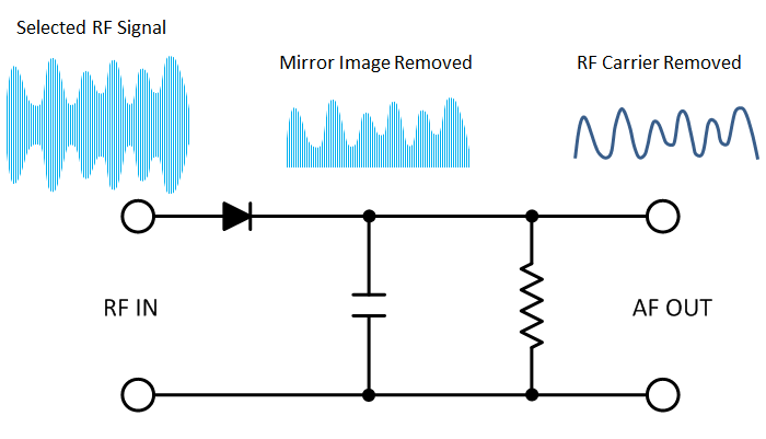
Once the mirror image of the information signal has been eliminated, the last step is to remove the RF carrier. To accomplish that a special circuit called an "RC Low Pass Filter" is needed that will pass the low frequency information signal but block the high frequency RF carrier. A simple RC Low Pass filter used in radio circuits is composed of a Capacitor and a Resistor connected in series. The cutoff frequency of the filter is determined by the simple equation below.
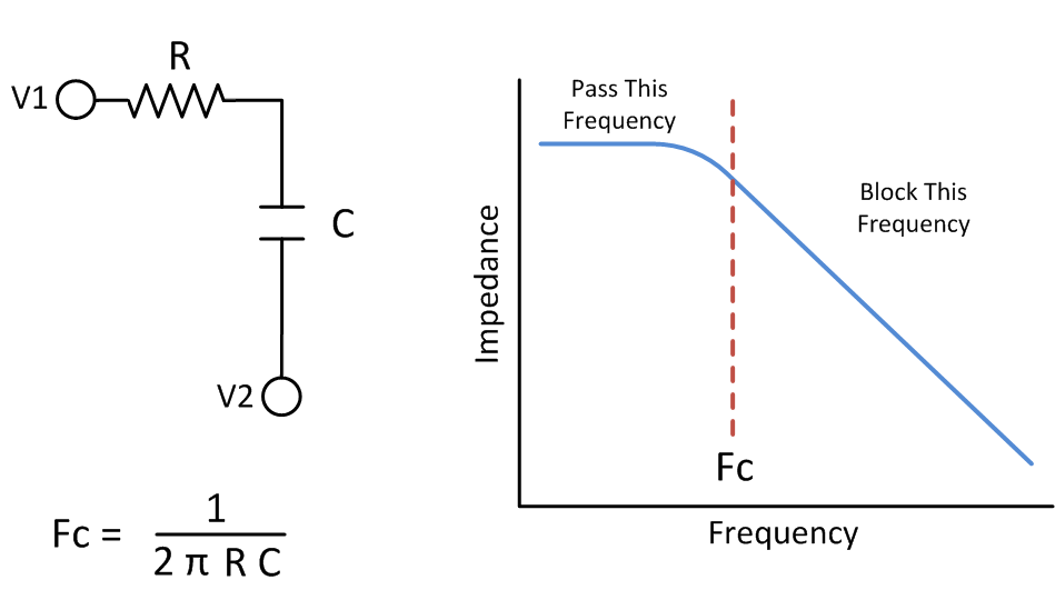
The resistor R in series with the capacitor C is the impedance of the radio looking toward the detector D and the tuner which is around 10K Ohms depending on the type of antenna coil used. The diode detector is used in the TRF, regenerative, and superheterodyne radios. It does not offer the highest sound quality but it is the simplest and least expensive. By assembling the building blocks just described, a simple TRF "crystal radio" can be constructed from just a few simple components as indicated in the schematic below.
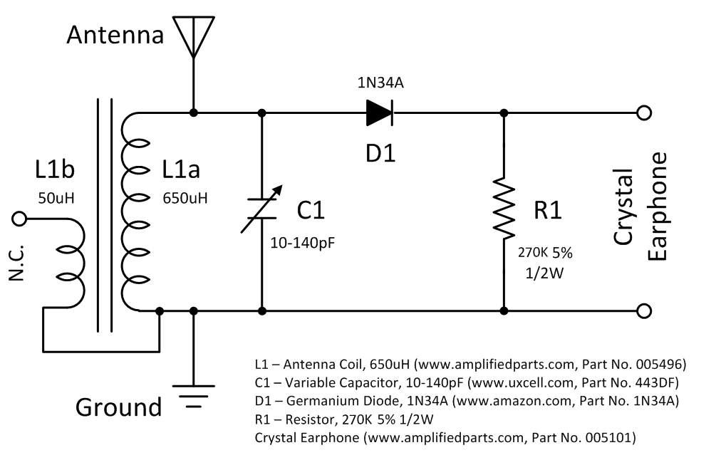
All components can be purchased from Amazon or from the indicated web site. The circuit above, with a good antenna, easily receives several AM broadcast stations within 550KHz and 1700KHz. The sensitivity and selectivity of this TRF radio can be improved by removing the AM detector, filter, and earphone from the L1a coil winding and adding an RF amplifier, AM detector, AF amplifier, and earphone/speaker to the L1b coil winding.
How This Radio Project Came To Exist
Radio Shack began offering 7 electronic kits in 1968 that included all parts, hardware, and instructions in a plastic box. The circuit offered in the kit was assembled by the customer on a perforated prototyping board. The popularity of these kits resulted in an expansion of the product line to 22 kits in 1969, but the perforated board was replaced with a plastic box, called a "pbox", that served as the shipping container, the project breadboard, and the project enclosure all in one. This "space age" pbox turned out to be much easier for young people to work with, reduced the cost of the kit, and made the finished circuit easy to use and interesting to look at.

By the early 80's, however, Radio Shack had become a struggling consumer electronics retailer and most of the kits and component parts were discontinued. While rummaging around in a local Radio Shack store after school I happened to find a 3 Transistor Short Wave Radio kit in a bargain bin, bought it, and assembled it with great pleasure.
I remember being amazed how well the radio worked using only the 10ft antenna wire supplied in the kit. Unfortunately, I do not remember what happened to the kit after it was completed. Recently I was designing and building a 40 meter SSB receiver and experimenting with software defined radio, and was describing to a friend the complexity of a modern radio receiver. It was then I thought of my old radio kit and how well it was able to operate with only three transistors and a 9V battery. Yes it was fiddly and hard to tune and you had to hold your hand in just the right place to stay in tune, but it could really pick out a long distance station. But then again, maybe my memory was off. I was a kid back then and it WAS the 80's so maybe it didn't really work as well as I thought. If only I could build it again. Alas, pbox kits had fallen into the abyss of the occasional outrageous eBay auction.
But... If I could find the original schematic perhaps it would be possible to redesign the kit to use silicon transistors. Maybe use some better knobs. I always felt like the original kit could have used some better knobs. And those original spring clips tarnished quickly. I began searching for information on the Radio Shack pbox kits and found a web site run by Steven Vornsand at www.sparktron.com that contained complete information on as many of the kits as were known to exist. A Google search turned up two companies that sold a compact variable capacitor (www.uxcell.com) and crystal earphone (www.amplifiedparts.com) that were critical components for the vintage-like operation of the radio design. So my first step was to reset the bias for the AF amplifier and AM detector which used old germanium transistors. Simulation and prototype construction revealed that the updated circuit with 2N3904 transistors worked slightly better than the expected performance of germanium transistors in the original circuit. The next step was to confirm that the 2N3904 could also be used in the regenerative RF amplifier section without change. Simulation and prototype construction also revealed a better than expected result. For tuning, I discovered that by eliminating the scaling capacitors from the original design the variable capacitor from Uxcell could then be used without having to change the winding dimensions of the air core tuning inductor. Last, I added an earphone jack (the AmplifiedParts earphone comes with a 1/4" plug) and some mini dual-position barrier strips to connect power, inductor, and antenna. Just for fun, I packaged up all the parts like a kit and assembled the final version presented in this article.
After building the radio I've successfully received WWV on 5, 10, 15, and 20 Mhz with good copy. I've picked up all the well-known short wave KW transmitters from around the globe. And I've picked up SSB on 7Mhz and 14Mhz. SSB can be received but the detector is not designed to clearly demodulate it. I remember that happening with the original kit.
I'm extremely happy with how the 3 Transistor Short Wave Radio looks and how well it pulls in distant stations.
How The 3 Transistor Short Wave Radio Works
The 3 Transistor Shortwave Radio in this article is a regenerative radio designed to tune from 2Mhz through 30Mhz depending on the tuning coil used by the operator. The schematic for the radio with the major building blocks highlighted is illustrated below:
Variable capacitor C5 and tuning coil L1 comprise the Tuning section. L1 is a fixed inductor wound according to the assembly manual for the frequency band of interest.
The RF Amplifier/AM Detector section is actually a Colpitts Oscillator with an added variable resistor R2 that serves as the regeneration control. Resistors R1 and R4 provide base voltage to Q1 so that it's collector is fixed at approximately 3V. This collector voltage was chosen so that the RF Amplifier/AM Detector will continue to operate properly as the 9V battery reaches the end of it's life. The large values of R1 and R4, and the bootstrap bias configuration they are connected in, were chosen so that the RF Amplifier/AM Detector will have a high input impedance which improves the selectivity and sensitivity of the radio. Capacitors C1 and C6 were included to bypass RF around resistors R1 and R5 respectively which improves the gain of the RF Amplifier circuit. The collector output of Q1 is fed back to the emitter of Q1 through capacitors C2 and C3. Normally this positive feedback would cause the RF Amplifier/AM Detector to continuously oscillate. However the regeneration control provides an adjustable amount of negative feedback at the emitter of Q1 that counteracts the positive feedback. By carefully adjusting the amount of negative feedback on the emitter of Q1, the circuit can be made to provide extremely high gain just before oscillation occurs, and at the same time remove most of the RF Carrier signal and the unwanted image of the audio signal. This behavior is the reason the regenerative radio works so well.
The AF Amplifier is a simple two-stage direct coupled Common Emitter amplifier for driving the crystal earphone. Transistor Q2 provides a gain of approximately 5 and together with R10 and C9 performs additional filtering of the carrier signal. Transistor Q3 provides a gain of approximately 100 (the transistor current gain at .5mA). Capacitor C11 is provided to bypass audio frequencies around resistor R12 and improve the gain of Q3. Together, Q2 and Q3 provide an additional gain of approximately 500 after the RF amplifier. The value of R12 was chosen so that the collector voltage of Q3 would be set at approximately 1/2 battery voltage which ensures that the Detector and AF Amplifier will continue to operate properly as the 9V battery reaches the end of it's life.
Capacitor C7 and resistor R6 are wired together as a simple RC Low Pass Filter to prevent RF noise at the RF amplifier from bleeding into the AF amplifier via the battery connections.
How to build the 3 Transistor Short Wave Radio
To build the radio described in this article, you will need the revised assembly manual I've created which include the design and layout changes I've made.
> Click Here to obtain the assembly manual <
Here's a few other things:
- The transistors for the radio can be purchased from Amazon.com or Radio Shack (assuming they are still in business in your area). I highly recommend the excellent Joe Knows Electronics semiconductor kit. It includes the transistors you need for this radio project and over 150 different types of transistors and diodes for just $22. And it includes a set of documents that are really good reading for the beginner. Check out www.joeknowselectronics.com. You will not be sorry.
Note: As of 2026, Joe Knows Electronics and Radio Shack are no longer in business. I have left the content here for historical purposes. - The resistors for the radio kit can be purchased from Amazon.com or Radio Shack. Radio Shack has a good selection of 1/4W resistors in a big 500 piece bundle for about $15.00 if you have a store nearby. Joe Knows Electronics also has a nice 800 piece package of 1% resistors for $12.00 if you don't mind ordering online. Joe's is a really good and well organized kit even if 1% resistors are a bit of tolerance overkill for this radio project.
- I strongly recommend ordering NP0 ceramic disk capacitors from www.mouser.com or www.digikey.com as they will far outperform most anything you can get on Amazon.com. The Joe Knows Electronics capacitor kit is an extremely good buy for every other capacitor at 645 pieces for $13.00. Don't bother with Radio Shack for capacitor kits as they are mostly junk values you will never use.
- I purchased several crystal earphones from www.amplifiedparts.com on Amazon.com and they work great despite the poor reviews. Whatever quality problem they had in the past seems to have been ironed out.
- The variable capacitor (and a lot of other rather old and interesting parts) can be found at www.uxcell.com which seems an unlikely domain for radio stuff but they do have a lot of radio stuff that's interesting. I've created a diagram of the variable capacitor >> here << that will help you figure out how to wire it in the radio.
- The case for the kit I built is a Hammond 1591GSBK ABS Project Box from Amazon.com with a piece of vector breadboard cut to fit on the top and spray painted with high temperature automotive flat red. I like the look of red on black, and the red color of the breadboard matched the red color of the original pbox kit. It's completely up to you how you want to house and color the kit you build.
- The knobs I used are Radio Shack knobs I've had in inventory for decades. Use anything you think is cool that will fit on the pot/varicap shafts.
- You will need to be creative on how you mount the variable capacitor on the vector board. I used a piece of 1/32" sheet metal cut to size with a Dremel tool grinding wheel and then drilled the holes to mount the variable capacitor with a power drill. Then I bent the end of it 90 degrees to form an L shape. This is the most challenging part. But I am sure you can overcome this minor obstacle being the resourceful person you naturally are.
- You will need to be creative on how you mount the tuning knob to the variable capacitor. The shaft on the varicap is only about 1/4" long so you will need something to extend it. I found a plastic cylinder with a hole drilled through it that was about 1" long at my local Ace hardware store. They have a really nice selection of odd hardware that is very useful. Again... be resourceful and look for a solution in unexpected places that will work. That's some of the fun of a project like this.
- The 2-position barrier strips are available from Radio Shack in a pack of four. These are a great value at the price so if your local Radio Shack hasn't yet been turned into a Sprint cell phone shop you should definitely buy all of the packs on the peg. I know I did.
When it comes to wiring, try to be as neat as I've indicated in the assembly manual. You don't have to be the world's best soldering artist but there's no good reason to do the work half-way. Go all out and make your radio look as good as you can. Here's what mine looks like from below:
In hopes of helping out, I've included a parts legend so that you can see where the components are supposed to go when the breadboard is turned over. When it comes to RF work, keep it short and keep it neat is good advice. Do what I did above and your radio will exceed your expectations.
One final note:
Any radio is only as good as it's antenna and the environment it is in. In my area, everybody and his extended family has a wireless router, 4 cell phones, three LCD TV's, and who knows what else making more electronic noise than a chicken coop surrounded by a family of foxes (Sorry, I couldn't help but include at least a little bit of classic Southern humor). A good antenna as described in the Assembly Manual is essential for getting the best performance from this radio project. I brought my radio out to rural Anacoco, Louisiana and attached a 10ft wire antenna to a clothes line, and received more stations than I had time to listed to. I was amazed at how well this little radio performs. If you don't know what a clothes line is, you probably don't live in rural Louisiana, and that's totally OK. Lets just say an electrically quiet environment also helps.
I hope you have as much fun working on this project as I did. Good luck and good listening!
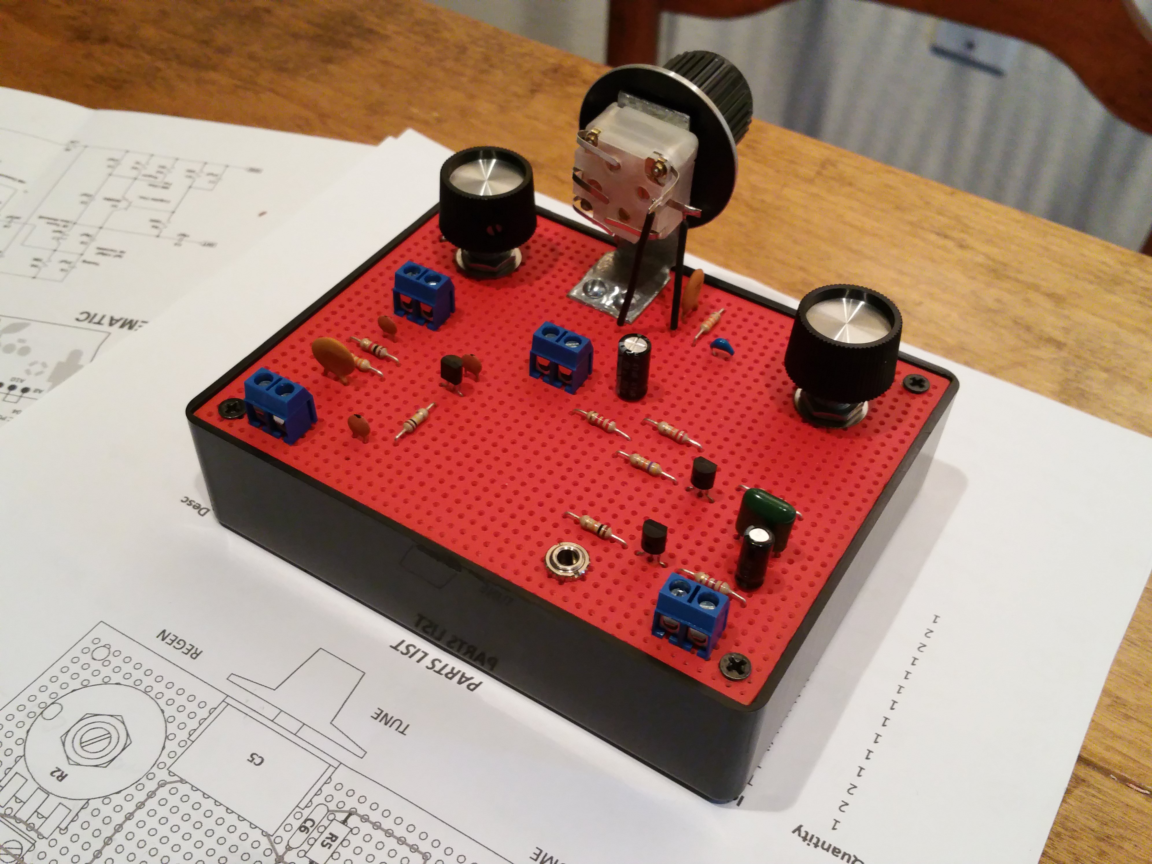
Build a Switched Mode Dual Variable Power Supply
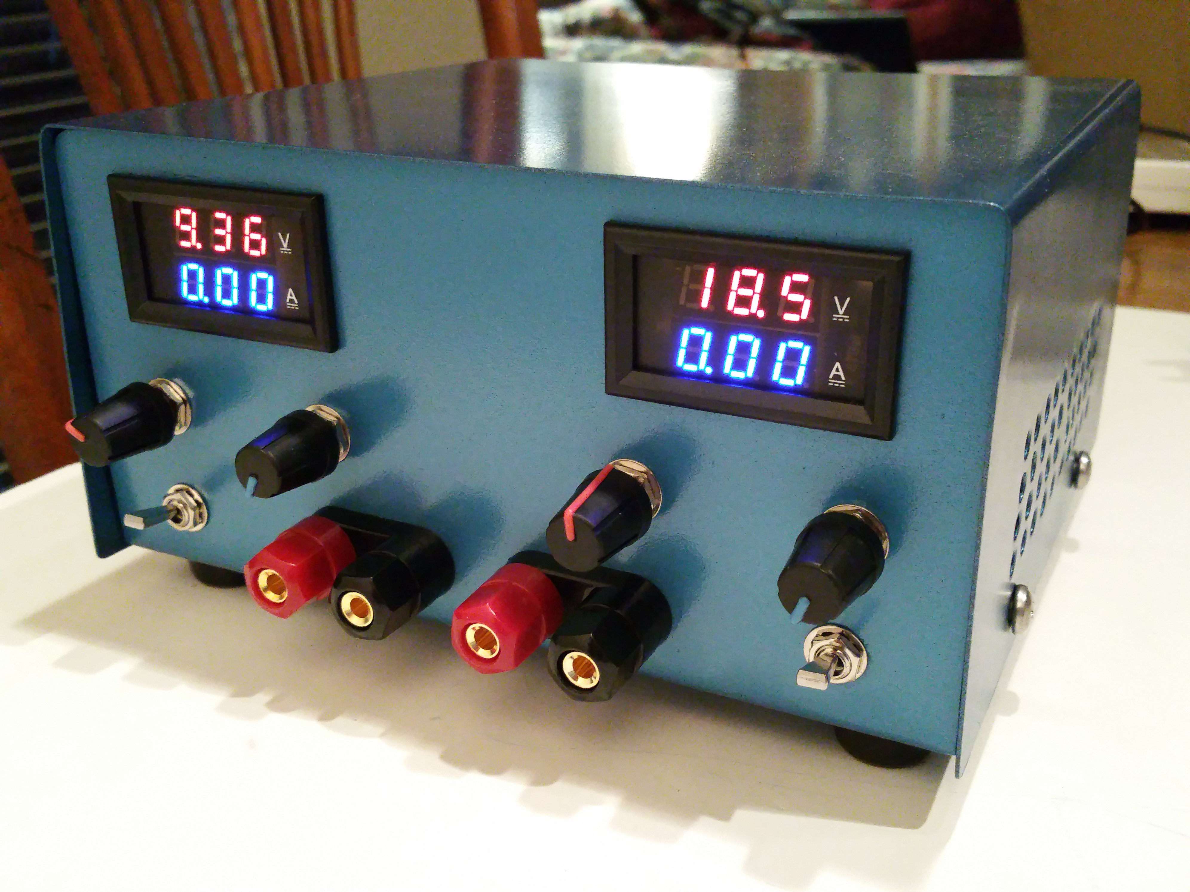
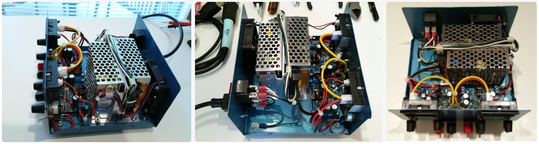
A variable power supply is one of the most important pieces of equipment to have on the electronics workbench. It's only a matter of time before the voltage or current required in a circuit isn't practical for battery power.
Bench-top variable power supplies available today are typically transformer-fed linear voltage regulators which are both simple and inexpensive to manufacture. However these supplies are also large, heavy, and inefficient for most of their output voltage range. Many linear designs cannot operate anywhere near their rated output current when large Vo-Vi is required, but for low power applications they provide stable and noise free output.
Switched-mode power supplies are more than 90% efficient through almost the entire output voltage and current range, require much less space for heat sinks and transformer cores (90% less in medium to high current designs), and are as much as 5 times lighter than an equivalent linear power supply. But these advantages come at the expense of ripple, noise, and transient response; the three parameters that linear power supplies excel at.
I was working with some high power LED designs recently that required 2.5V to 9V and forward current between 1 Amp and 2 Amps. My LM317-based lab supply couldn't run more than a few minutes without tripping the thermal overload due to VI and Pmax limitations. This was a pretty hefty supply but it was getting too hot to operate reliably. So I decided to build my own 100W dual variable switched supply that could drive 2 Amps at an output voltage between 1V and 20V.
I wanted the regulation specifications to be competitive with the LM317 but my application did not require an extremely low ripple/noise figure. Current limiting and overload protection were important so independent voltage and current adjustments were required. And it would be nice to include a V/I meter for each supply for convenience.
This project will illustrate how to construct the 100W dual output switched mode variable power supply I have for about $150 using off-the-shelf modules and a prefabricated enclosure available on amazon.com or ebay.com. This power supply is compact, weighs less than 3 lbs, and deliverers professional appearance and performance competitive with commercial switched power supplies.
I've used this supply for a lot of heavy duty circuits including a DC motor controller and a 50W prototype audio amplifier with great results. I would not recommend this supply for precision Op-Amp or Radio Frequency circuits but for just about everything else it has worked really well.
Review the Power Supply Design
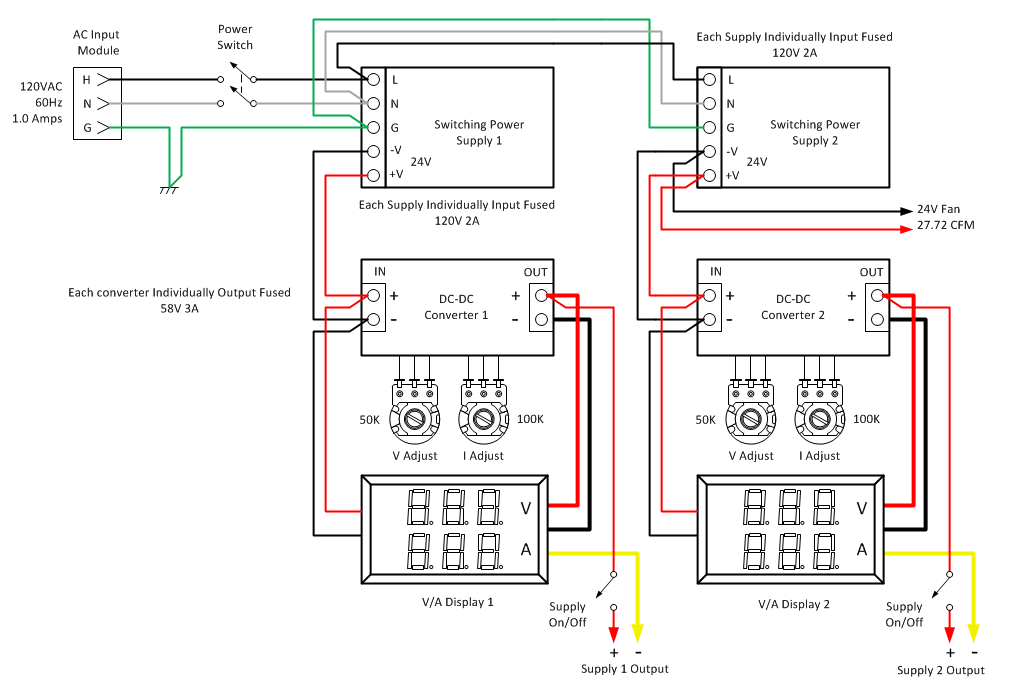
The Switched Mode Variable Power supply was designed using off-the-shelf modules that could be wired together using simple tools and basic soldering and wiring techniques. Two modules require modification so that front panel controls can be used instead of the PCB mounted multi-turn potentiometers included with the modules. These modifications are covered in a later step.
Power Supply Specifications
Input: 120VAC (+/- 15%) 60Hz 1A Full Load
Output 1: 1.2V - 20V @ 2 Amps
Output 2: 1.2V - 20V @ 2 Amps
Load Regulation: 0.5% Full Load
Line Regulation: .001% Full Input Range
Noise/Ripple: 20mV RMS, 100mVpp
General Circuit Description
AC power is connected to the supply via an IEC 320-C13 AC input module. AC safety ground is bonded to the power supply case and feed through to switching power supplies 1 and 2. The case of the power supply is grounded to the AC mains circuit. DC output ground is electrically isolated and independent of the AC mains ground.
Switching power supplies 1 and 2 are energized and de-energized through an illuminated DPST power switch. These supplies provide the constant 24V DC needed for DC-DC converters 1 and 2, the cooling fan, and the V/I displays. DC-DC converters 1 and 2 provide controlled output voltage and current to the power supply binding posts.
The output voltage and current set points are determined by two 50K Ohm and two 100K Ohm single-turn potentiometers. The DC positive power connection can be disconnected from the circuit by flipping the output power switch to the off (Down) position.
Two panel meters provide direct readout of the voltage set point and the current being consumed by the circuit attached to each power supply. The panel meters use a shunt type current sensor inline with the DC ground conductor. Power for each meter (< 20mA each) is taken directly from the 24V switching power supplies.
All power supplies are current and thermal overload protected and include last resort short circuit protection via fuses on switched power supply AC input and converter DC output. Cooling for the power supply is forced air via a 27 CFM fan using 24V @ 100mA drawn from switching power supply 2.
Design Tradeoffs
In order to keep total cost around $150, single-turn potentiometers were used instead of precision multi-turn potentiometers. Setting the output voltage is easier with 10-turn precision pots but a well made set would have increased the cost of the supply by $40. I decided to live with the fiddly nature of a general purpose single-turn pot for setting the output voltage. My applications do not require exact voltages. Close enough is good enough.
In order to keep costs low and simplify module wiring, I did not use DC-DC converters with an external voltage sense feature. This results in a slight degradation in load regulation (0.5% instead of 0.1%) due to the current shunt used in the current meter.
The 60mm x 60mm fan I used is overkill for this design and a bit louder than I would have liked. Lower CFM fans from Delta Electronics were non-stocked at Mouser so I decided to accept the overkill. With the supply installed on the instrument shelf I hardly notice the fan noise among all the other fan noise going on in the lab.
The current limit control is usable for only about half of it's range due to the 5A current rating of the DC-DC converter. I could have used two resistors to scale the current control to use the full rotation but did not feel the wiring complexity was worth the effort. I usually start with minimum current on a new circuit and slowly increase the current limit until a stable output voltage is achieved. I might add the scaling resistors at a later time if I think it's needed.
A full size PDF file for all Power Supply diagrams and parts list can be downloaded >>> HERE <<<.
Review the Parts List
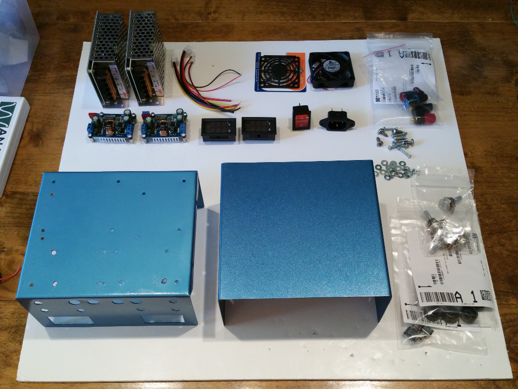
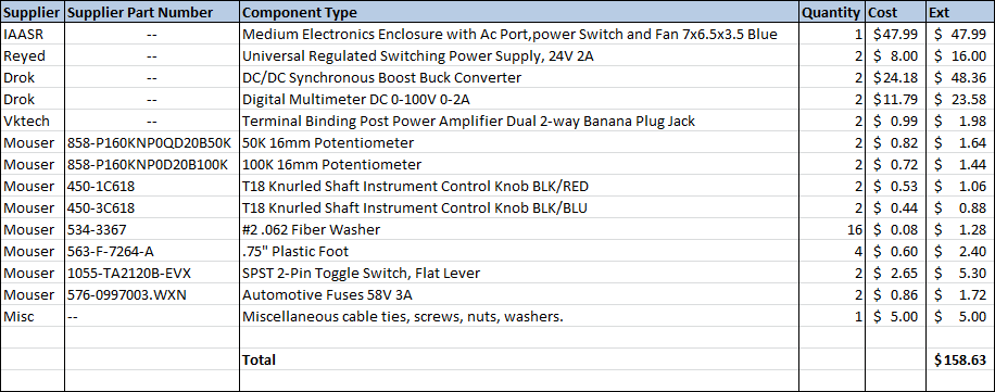
Obtain the parts listed for the power supply project. Everything can be purchased from Amazon, eBay, and Mouser as of August 2015. All prices are current as of August 2015.
I keep an inventory of plastic cable ties and a variety of screws, nuts, and washers. I used a few of these in the finishing of the power supply and didn't list them in the parts list because their single unit cost is extremely low. Have on hand some 4" cable ties and a few pieces of #6 and #10 screws/nuts/washers.
With respect to the IAASR SimCase product there are a number of options available on the iaasr.com website. Be sure to choose the color you want, select fan/power/ac-input, and choose the 24V fan option.
Please Note: I have no business relationship with any of the vendors in my parts list. Nothing of financial value was exchanged for my recommendation. None of the above vendors provided compensation of any kind during the creation of this project. I will not be compensated in any way if you choose to build this project or purchase components from any vendor I recommend. I simply had a good experience with the vendors I recommend and believe you will too.
A full size PDF file for all Power Supply diagrams and parts list can be downloaded >>> HERE <<<.
A Word About Electronics Enclosures

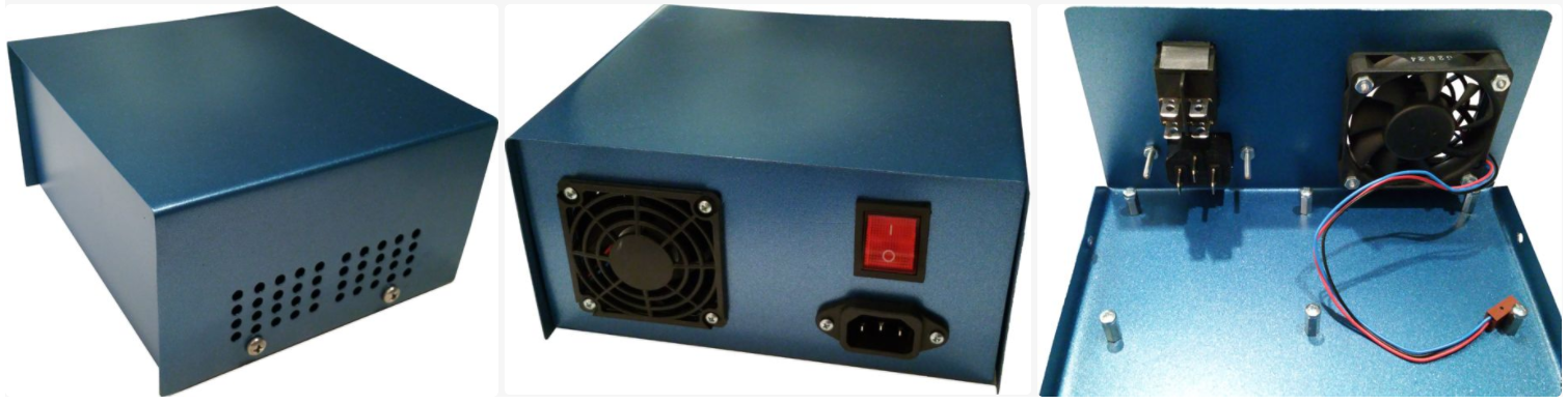
NOTE: As of 2026 IAASR is no longer in business. I have left the content here in place for historical reasons. I have provided detailed construction drawings for the case in the "Prepare the Enclosure" section below.
I love to see a useful project professionally finished in a nice enclosure. A well designed enclosure improves the durability and appearance of a DIY project and enhances the "I made that" pride in craftsmanship a builder earns from the work. However, many builders have the following complaints with the enclosure products available on the market today:
1. Project boxes cost more than the value they add, and sometimes more than the parts they enclose.
2. Poking holes of various shapes and sizes in an enclosure is hard work. If not done properly, the appearance of an expensive enclosure can be destroyed.
3. Designing the front and back panel layout is time consuming and not as much fun as designing and building the circuit.
4. It's difficult to find an enclosure that is the right size and shape for a particular type of project.
When I started looking for an enclosure for the dual switch-mode power supply project, I was shocked at the prices manufacturers were asking for a simple project case. The basic grey on grey cabinet without a single hole cut in it was $100 and up! If I was going to spend that kind of money, I better have a fully equipped machine shop to do the job right. But then the sizes available were either too large or too small, too deep or too tall. I didn't want unpainted aluminum or battleship grey. None of the manufacturers in Mouser or Digikey had anything that fit my design in an affordable, easy to build way.
While searching through Amazon and eBay I happened to discover IAASR and their line of SimCase and HexCase enclosures. These are purpose-built enclosures with holes already cut and parts already installed for specific use-cases. When I saw the IAASR SimCase I said "That's exactly what I need!". The SimCase product is designed by IAASR to house a DIY power supply. It includes an EMI shielded mild steel enclosure, the AC input module, an illuminated AC power switch, a fan, and ventilation holes validated with thermal analysis software... for $49. That's a layout I didn't have to design, parts I didn't have to research and order, and holes I didn't have to cut which would save me a huge amount of time. IAASR offers their enclosures in 5 standard colors and 15 custom colors which means your project can look cool like you imagined it would instead of like a low-bid government job.
But that's not all. I contacted Shiraz Macuff, CEO, about the front panel design. He says, "Send me a layout and we'll cut the holes before we ship at no extra charge". That's service you can only get when you order quantity 10,000 from any other manufacturer. I ordered quantity one from IAASR. It turns out that IAASR is disrupting the enclosure market with purpose-built products that save time, add value, and can be mass-customized to meet the requirements of the DIY, prototype, and small-medium volume manufacturer. IAASR enclosures can make your DIY project seem more like a professionally designed kit. And you don't have to worry about accidentally mutilating your enclosure with a power drill.
In this article, I am including the design drawings and assembly steps for a generic enclosure. But I strongly encourage you to use the IAASR SimCase product indicated in the parts list instead of trying to make do with the generic cases sold elsewhere. You will enjoy the building experience much more when you can focus on the assembly work and not have to put up with the dull, dirty, and sometimes dangerous fabrication work. Shiraz and his team can save you a lot of time.
Please Note: I have no business relationship with IAASR of any kind. Absolutely nothing of any financial value (money, product, gift cards, work for free, etc.) is exchanged between IAASR and I (or anyone associated with me) if you choose to buy from them. I'm recommending them because I like their product and the support I have received has been excellent. IAASR saved me a lot of time building this project and I think you will be happy with them as well.
Prepare the Enclosure
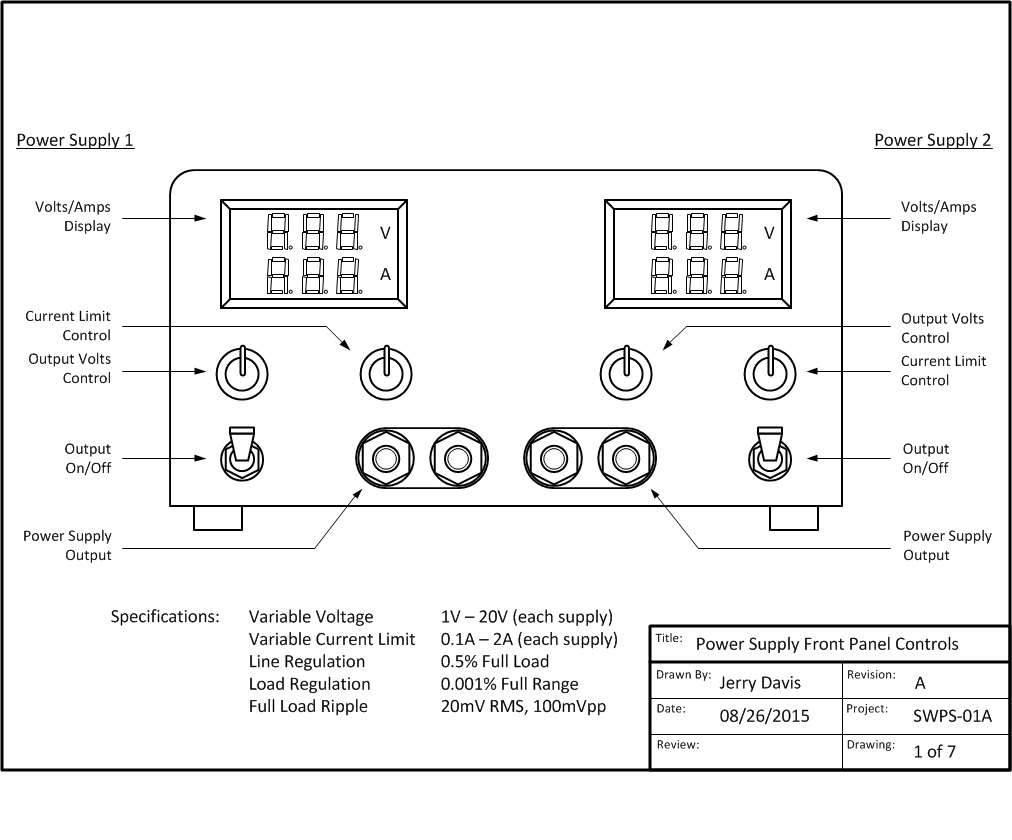
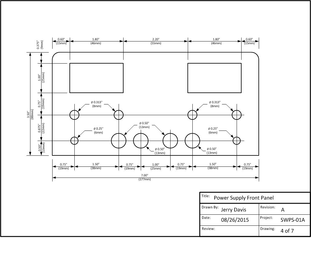
The power supply project described in this article requires an enclosure with the following minimum dimensions:
7" Wide x 3.5" High x 6" Deep
Although the enclosure can be constructed of any rigid material (plastic, aluminum, etc.) I recommend using a material that can provide some EMI shielding and AC ground fault protection. In this design I used a painted steel enclosure from IAASR which had the holes cut and AC input, AC switch, and fan already installed. I removed the components for illustration purposes showing the product being fully assembled.
Attached below are the detailed shop drawings needed to fabricate the enclosure front, back, and bottom panels.
The shop drawings are full-scale and can be used as a template for transferring the layouts to the enclosure. When cutting holes, I strongly recommend protecting the panels with two layers of painters tape to prevent accidental scratches and tool marks from marring the finish.
If using a power drill for round holes, be sure to use a thick piece of wood at the back to avoid bending/cracking the panel and to act as a drill stop. Square openings can be cut and smoothed out with a Dremel tool cutoff wheel. Curved openings in steel can be rough cut with a Dremel tool cutoff wheel and finished up with a Tungsten Carbide cutter.
If you purchase the SimCase enclosure from IAASR you can skip this step.
A full size PDF file for all Power Supply diagrams and parts list can be downloaded
>>> HERE <<<.
Install the Case Feet
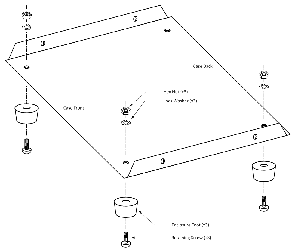
1. Remove the plastic case feet from the package and verify all mounting hardware is present.
2. Install three plastic feet as shown in the illustration above. Do not install the left rear foot (next to the AC input module position) yet.
3. Cut one piece of green #18 AWG wire 2" long, and one piece of green #18 AWG wire 4" long. Strip and tin 1/4" from each wire end.
4. Insert one end of the 2" and 4" green wire into a #8 Ring Terminal and solder the wires to the terminal.
5. Solder a 0.25" Female Quick Disconnect connector to the free end of the 2" green wire.
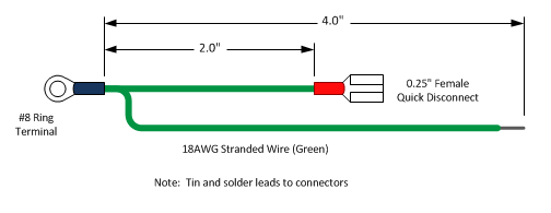
4. Scrape off the paint inside the case around the foot screw hole so that the ground cable ring terminal makes metal-to-metal contact with the case.
5. Install the last plastic foot as shown in the illustration below making sure that the ground cable ring connector is installed first, then the lock washer, and finally the hex nut.
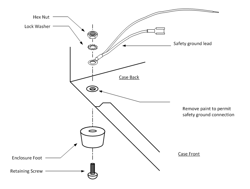
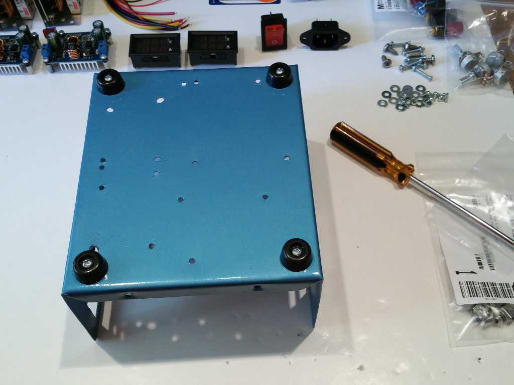
Install the AC Input Module
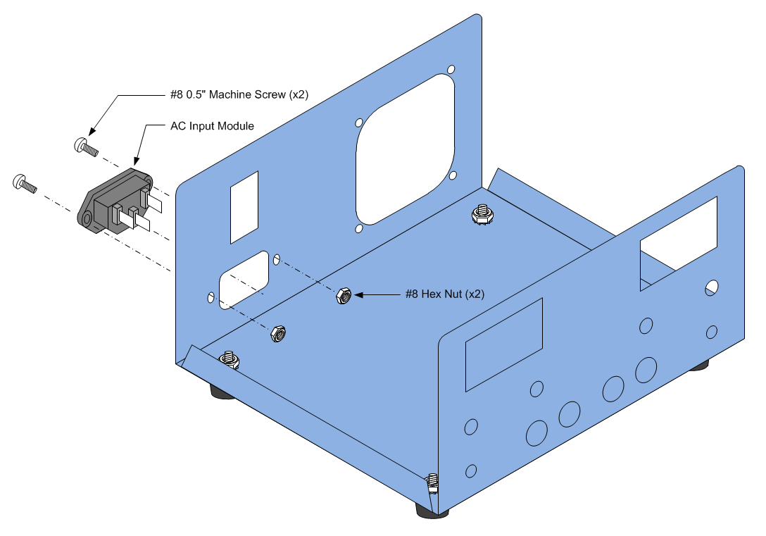
Note: If you purchased a case from IAASR the AC Input Module is already installed. Skip to the next step.
1. Insert the AC Input Module oriented as illustrated in the diagram above.
2. Fasten the AC Input Module to the case with two #8 machine screws and hex nuts.
3. Firmly tighten the machine screws but do not over-tighten.
For reference, the AC Input Module datasheet is included <<HERE>>.
Install the AC Power Switch
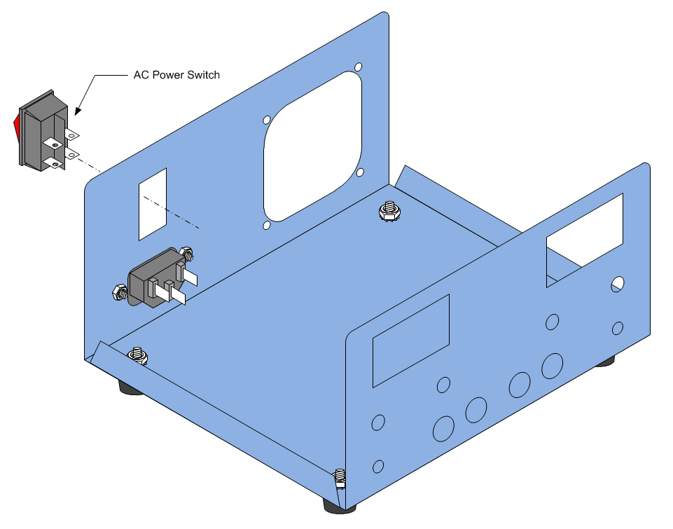
Note: If you purchased a case from IAASR the AC Power Switch is already installed. Skip to the next step.
1. Insert the AC Power Switch as illustrated in the diagram above.
2. Push the AC Power Switch into the case cutout until the top and bottom retaining clips snap into place.
Install the Cooling Fan
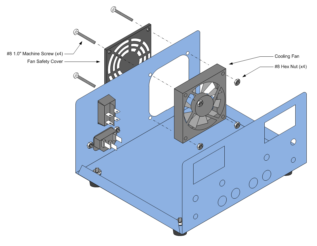
Note: If you purchased a case from IAASR the Cooling Fan is already installed. Skip to the next step.
1. Hold the fan cover against the outside fan opening and thread a single #8x1" machine screw through the cover and into the case.
2. Determine the direction of fan flow from the datasheet and orient the fan so that it's exhaust side is facing the fan cover.
3. While holding the screw in place, slide the fan (wire leads facing up) over the machine screw and thread a #8 hex nut onto the screw until both the fan cover and fan are held loosely against the case.
4. Line up the cover and fan so that each machine screw can be threaded through the cover and fan.
5. Insert the remaining three machine screws through the cover and fan.
6. Thread a #8 hex nut onto each machine screw until all four corners of the cover and fan are held loosely in place against the case.
7. Tight each machine screw until firm. Do not over-tighten.
For reference, the fan datasheet is included >>> HERE <<<.
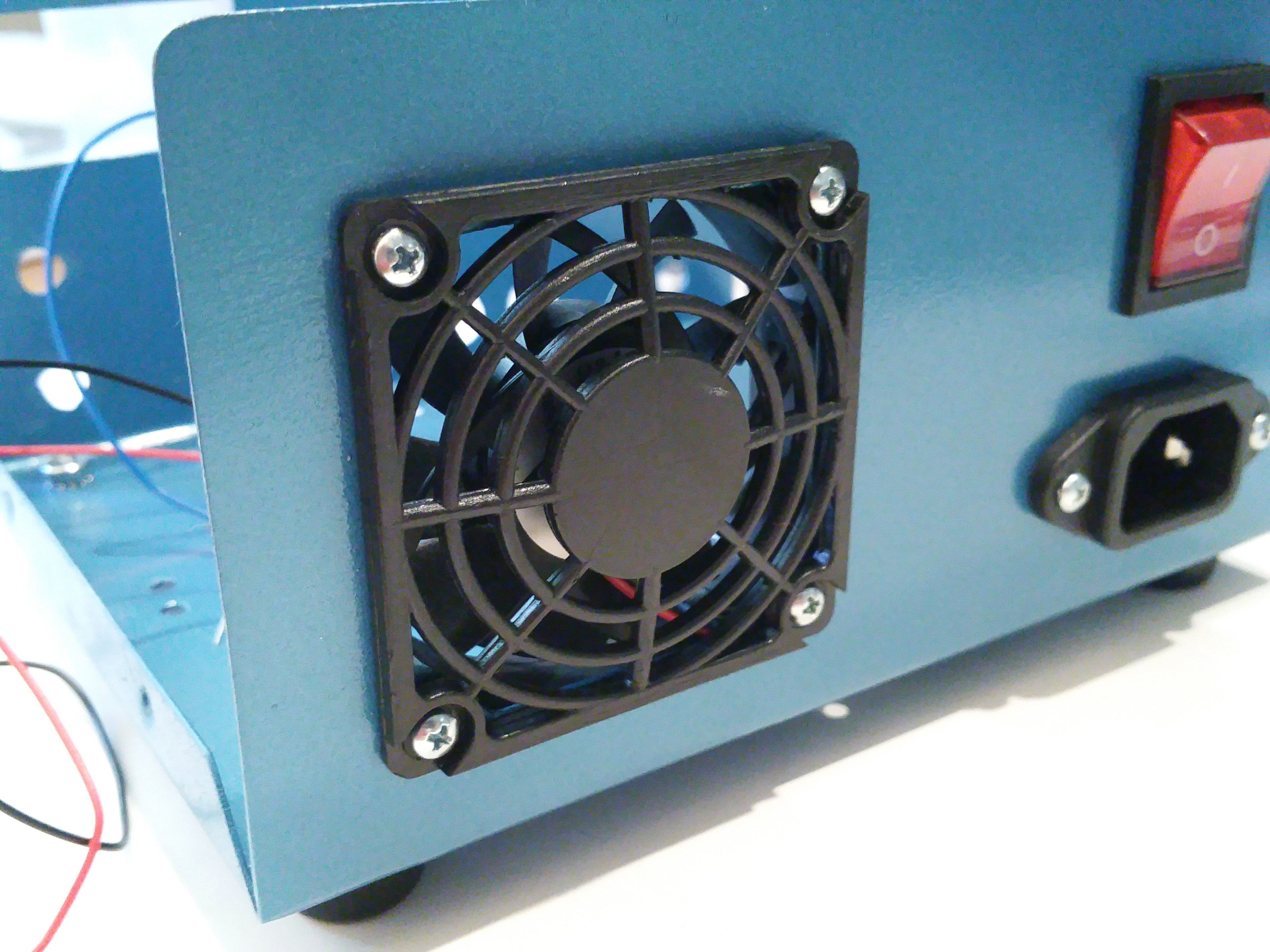
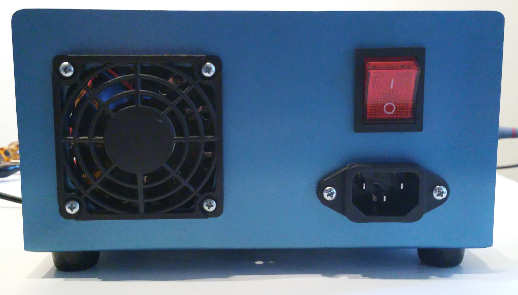
Wire AC Input, AC Switch, and Ground
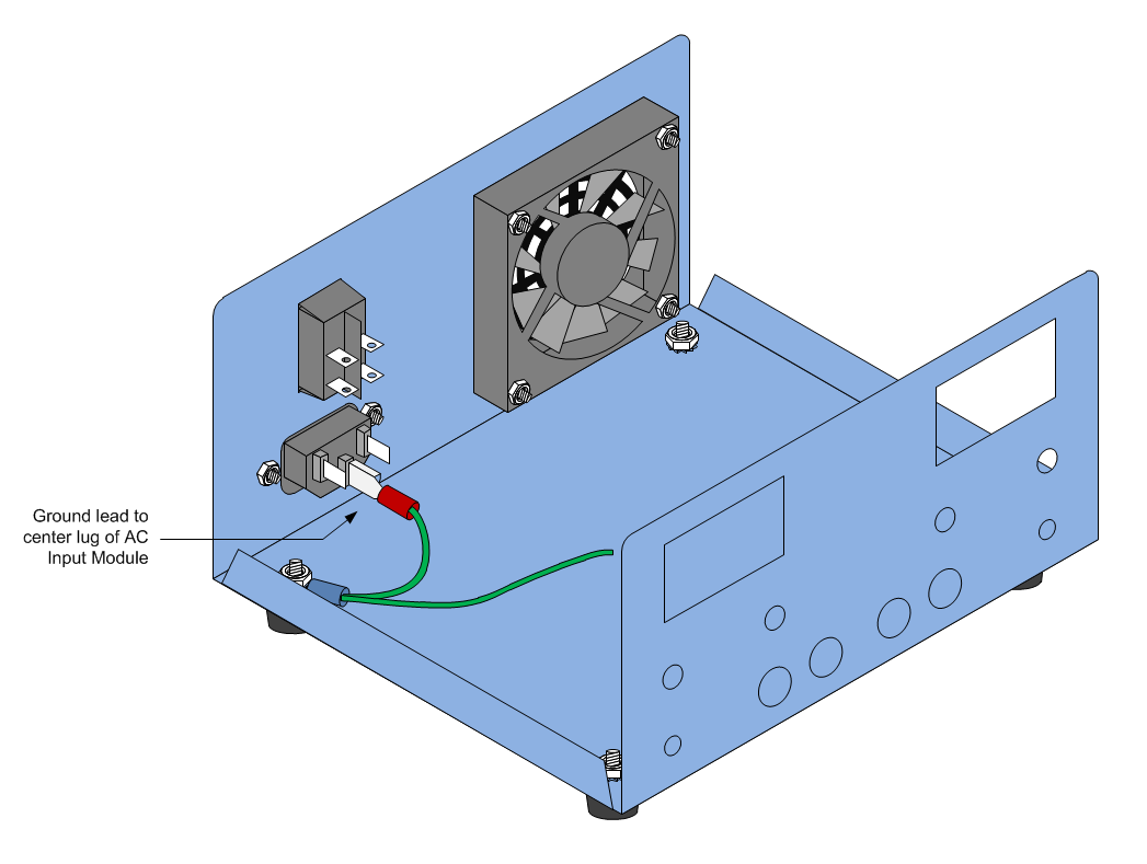
1. Connect the ground lead quick disconnect to the center lug of the AC input module as illustrated in the diagram above.
2. Cut one piece of white #18 AWG wire 1.5" long, and one piece of black #18 AWG wire 1.5" long. Strip and tin 1/4" from each wire end.
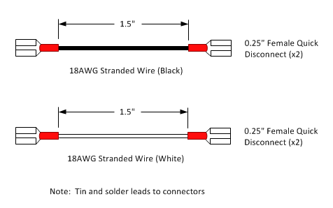
3. Solder two 0.25" Female Quick Disconnect connectors to the black wire.
4. Solder two 0.25" Female Quick Disconnect connectors to the white wire.
5. Connect one end of the black lead to the left lug of the AC input module. Connect the other end to the bottom left lug of the AC Power switch. Refer to the diagram below to verify that the black lead is connected properly.
6. Connect one end of the white lead to the right lug of the AC input module. Connect the other end to the bottom right lug of the AC Power switch. Refer to the diagram below to verify that the black lead is connected properly.
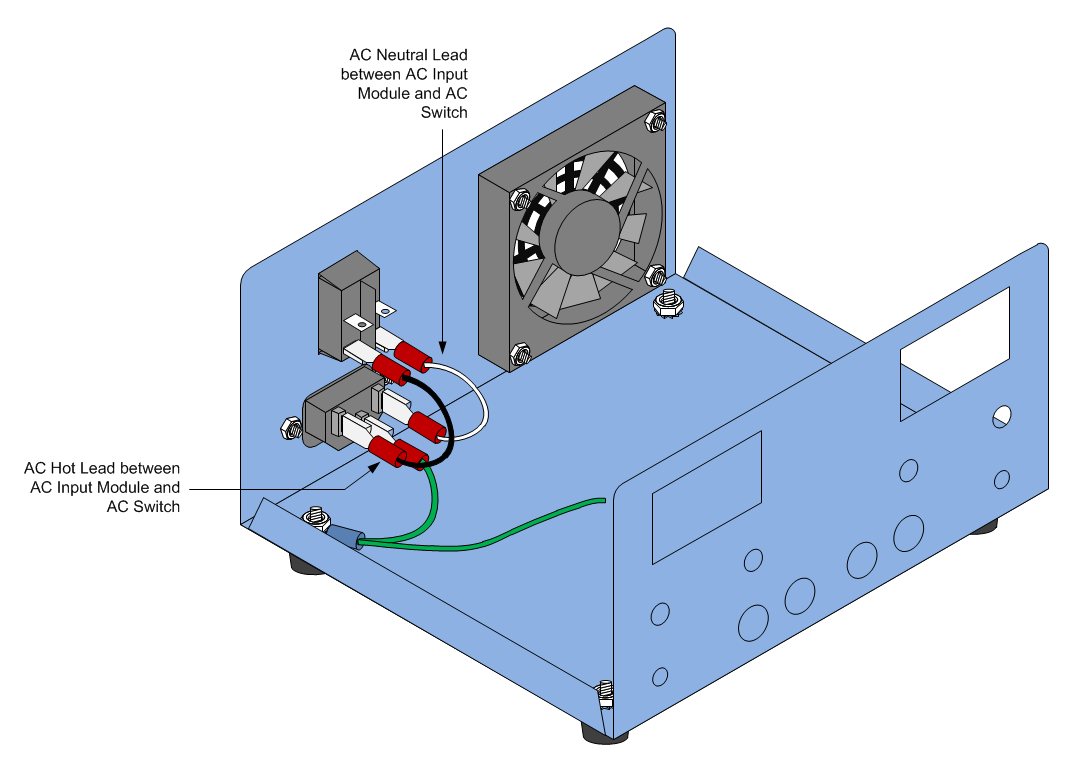
Install Front Panel Binding Posts
The binding posts from Vktech are ruggedly constructed and include a lot of mounting hardware which makes them a good value for the money. However the center conductors are about 1/2" longer than necessary which can waste a lot of space in the cabinet. To keep the supply compact, the binding posts must be modified as indicated in the above diagram and the following steps:
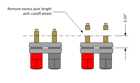 1. Remove all the hardware from the binding post and pull off the rear plastic insulator.
2. Unscrew the Red and Black post caps several turns and push down firmly from the end each cap to make sure the center conductor is seated all the way down on the front plastic insulator.
3. Using a Sharpie pen and a ruler, measure and place a mark on the metal center conductors 1/2" from the front plastic insulator (refer to diagram above).
4. Using a cutoff wheel and a Dremel tool, cut through the metal center conductors at the marks to remove the top portion of the center conductors (refer to diagram above).
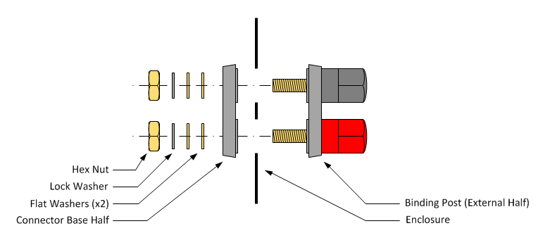
5. Insert the front portion of the binding post into the case (refer to above diagram).
6. Slide on the rear plastic insulator, followed by two flat washers, and a lock washer on each center conductor (refer to above diagram). All hardware is included with the Vktech binding posts.
7. Thread a hex nut onto each binding post and hand tighten while sliding the insulators back and forth until they are seated properly in their holes. Do not tighten fully yet.
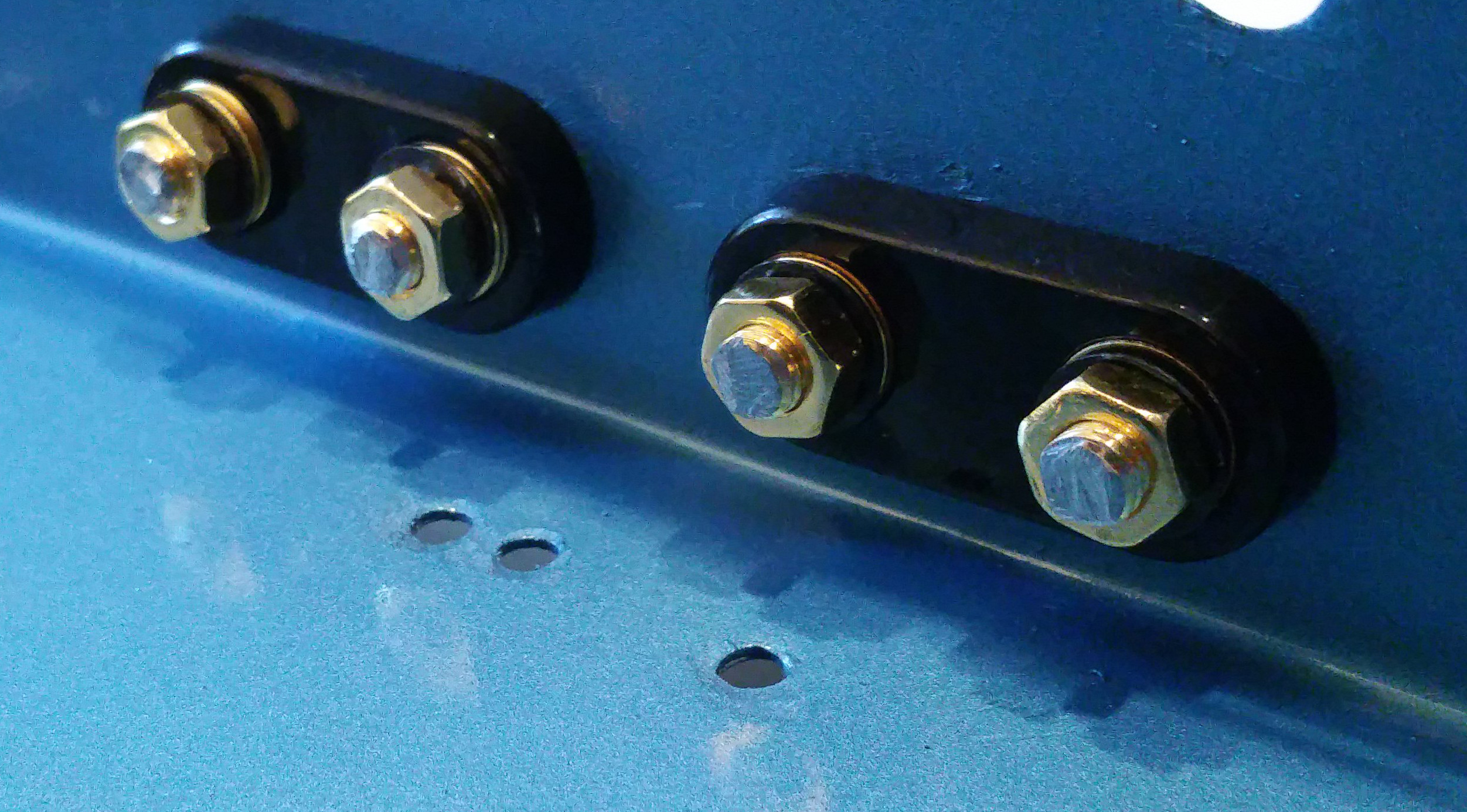
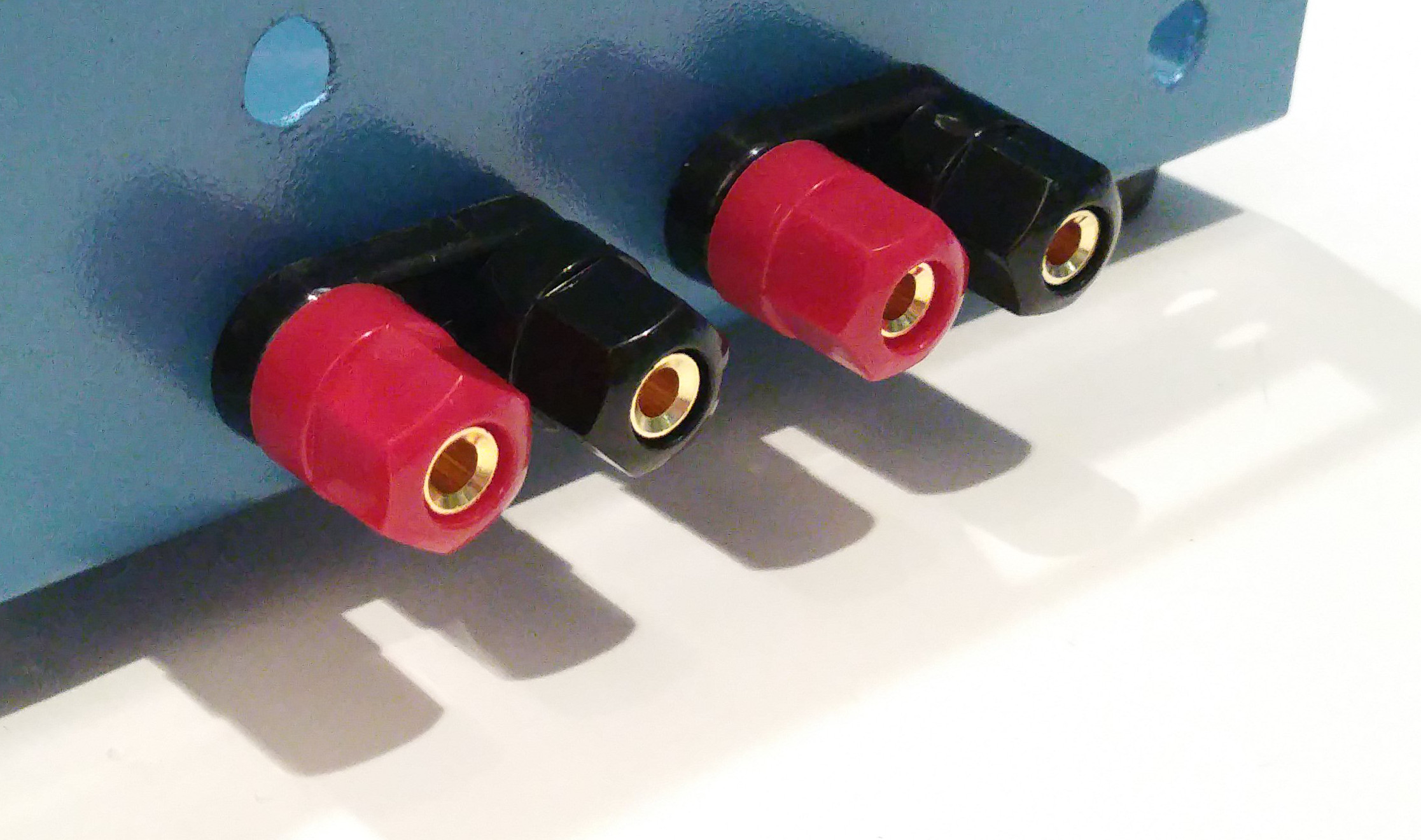
Install Front Panel Output Switches
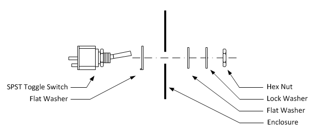
1. Remove the outer hex nut, lock washer, and flat washers from the SPST toggle switch.
2. Hand tighten the inner hex nut until snug against the switch body.
3. Install the large flat washer with the tab facing toward the switch body as illustrated in the diagram above.
4. Insert the SPST toggle switch into the bottom left hole in the front panel.
5. Orient the SPST toggle switch so that the two solder lugs are closest to the bottom of the enclosure as indicated in the diagram above.
6. Install the small flat washer onto the toggle barrel at the front of the enclosure as indicated in the diagram above.
7. Thread the hex nut onto the toggle barrel until hand tight.
8. Hold the switch body in position and firmly tighten the hex nut. The switch body should not move when the toggle switch is operated. If it does, tighten the hex nut until the switch body does not move.
Repeat the above for the SPST toggle switch on the bottom right of the front panel.
For reference, the SPST toggle switch datasheet is included >>> HERE <<<.
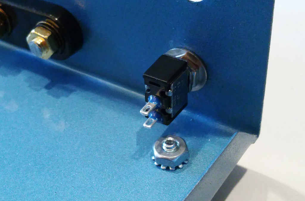
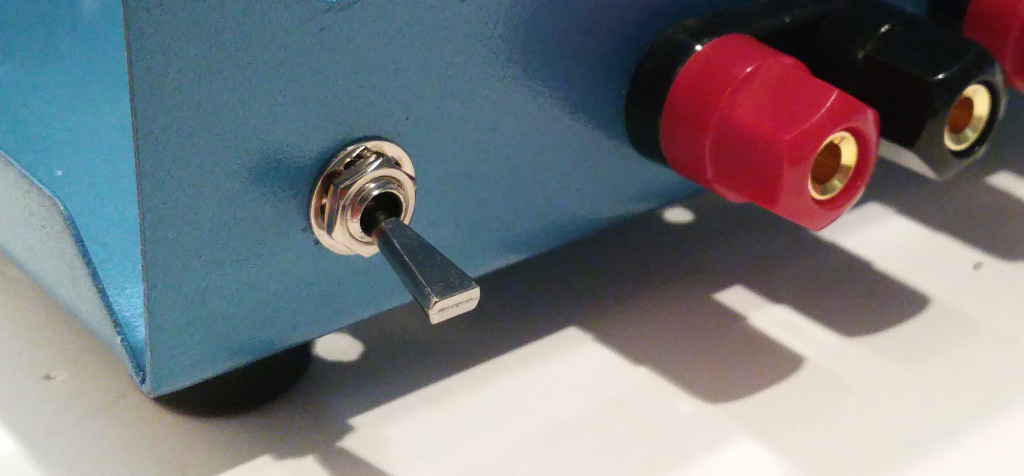
Install Potentiometers
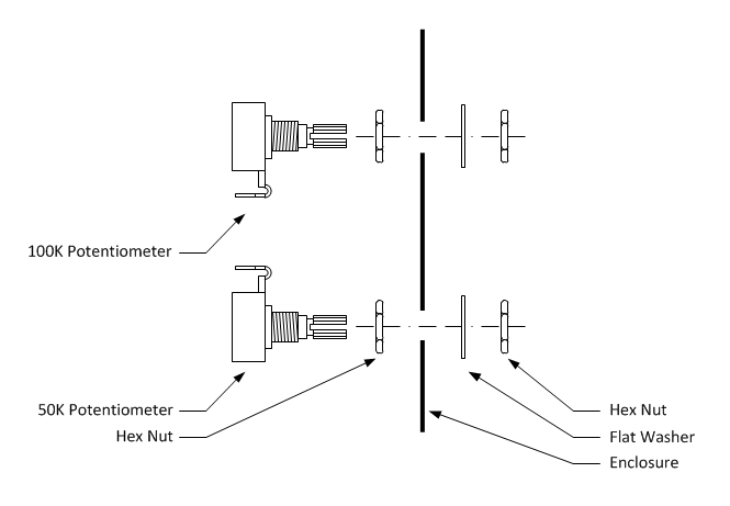
1. Thread a hex nut onto two 50K Ohm potentiometers and hand tighten until snug.
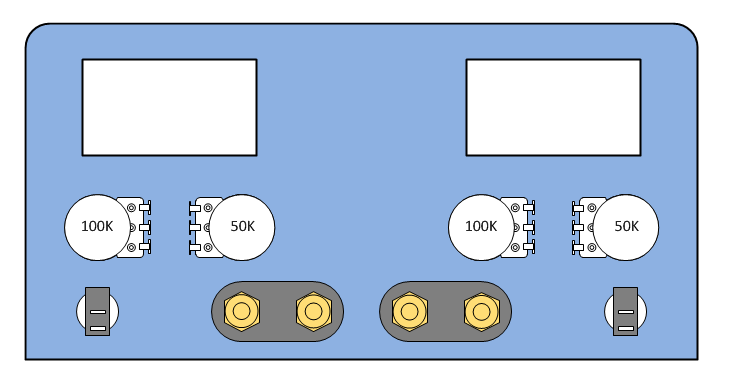
2. Insert the 50K Ohm potentiometers into the positions indicated in the above diagram.
3. Install a flat washer onto the 50K Ohm potentiometer shafts.
4. Thread a hex nut onto the 50K Ohm potentiometer shafts until hand tight.
5. Hold the potentiometer body in the position indicated in the above diagram and firmly tighten the hex nut. The potentiometer body should not move when the shaft is turned throughout it's full range of motion. If it does, tighten the hex nut until the potentiometer body does not move.
Repeat the above steps with the 100K Ohm potentiometers.
For reference, the potentiometer datasheet is included <<< HERE >>>.
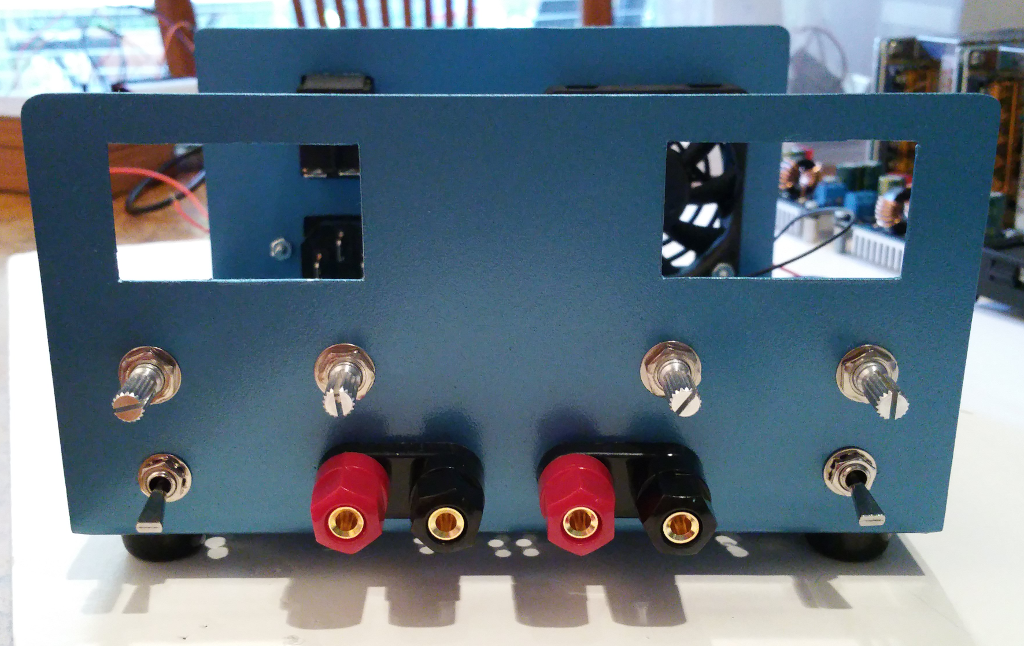
Install V/I Meters
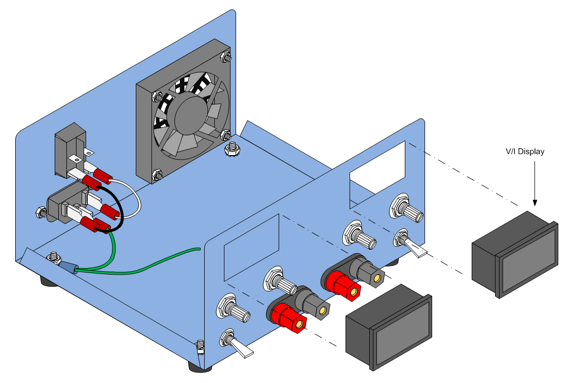
1. Insert the V/I displays half way into the cutouts provided.
2. Using fingertips or a screwdriver, depress the plastic retaining clips on the display bezel so that they clear the panel cutout.
3. While keeping the plastic retaining clips depressed, press the display into the cutout until the clips snap into place. Use care not to bend the panel while installing the displays.
Note: On some V/I displays the plastic retaining clips are too thick or too rigid to allow the display to be easily installed without bending the front panel. The best solution is to trim some of the plastic from the retaining clips until the display can be installed with reasonable force.
Note: On some displays the plastic retaining clips are too far back from the front bezel which causes the displays to fit loosely in the front panel. The best solution is to hold the display against the front panel while running a small bead of hot glue along the left and right side of the display (inside the case). Use caution to avoid getting glue on the outside front panel.
Install Control Knobs
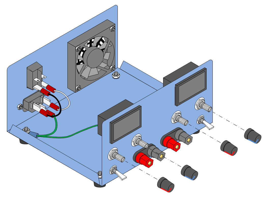
Insert the Red and Blue control knobs onto the front panel potentiometers as indicated in the above diagram.
The enclosure is now complete with all attachments and controls. The next section will describe how to install and wire the power supplies and converters.
For reference, the knob datasheet is attached >>> HERE <<<.
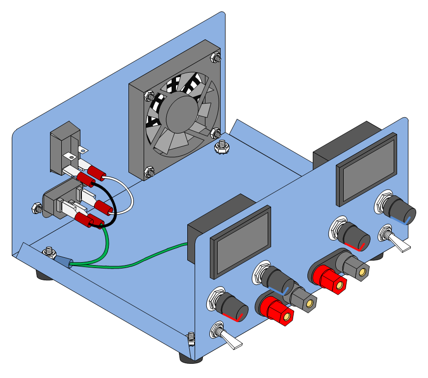
Prepare the DC-DC Converters
The DC-DC Converters used for this project accept a wide range of input voltages (5V - 32V) and convert that to a variable voltage between 1V and 20V with adjustable current limit between 0.1A and 3A. The DC-DC converters are operated in step-down switch-mode from a 24V DC input. The DROK converters are compact, easy to use, and >95% efficient for most of their range.
Adjustment of the output voltage and current limit is accomplished with two multi-turn trimmer resistors. In order to bring these adjustments to a potentiometer on the front panel, it is first necessary to remove the trimmer resistors. The quickest way to do that is to carefully cut them off of the board with a small pair of wire cutters. This might seem extreme but the PCB is very thick and the trimmer resistors are soft and easy to cut through. When the trimmer resistor body is removed, there will be three small component leads sticking up that can be easily desoldered. I believe this method is faster and results in less chance that pads and traces will be damaged from excess heat. I used the cut and release method on both converters with no problems. If you have a vacuum powered desoldering station by all means give that a try. Start with DC-DC Converter #1:
1. Notice that on each board the parameter that the trimmer resistor adjusts is indicated in white letters. On a blank piece of paper, draw an outline of the board and make a note of which trimmer is the voltage adjustment (CV) and which trimmer is the current adjustment (CC). On the DC-DC converters used for this project, the voltage trimmer was on the outside of the board and the current trimmer was next to the voltage trimmer.
2. Starting with the outside trimmer, use a small pair of wire cutters to cut a small groove into the outside corner of the trimmer body. Use one hand to hold onto the trimmer resistor while cutting with the other hand. Use only the force necessary to keep the wire cutter blades in contact with the trimmer body. Let the scissor action of the wire cutters do the work. The goal is to cut through the plastic body of the trimmer. Don't try to cut too much at one time.
3. When the corner gap is deep enough, begin cutting a groove into the adjacent corner next to the inside trimmer. When the second groove is deep enough, cut through the side of the trimmer body. There may be a crunching sound as the wire cutters reach internal ceramic components. Do not be concerned. Only the trimmer is being damaged.
4. Starting with the opposite outside corner of the trimmer, begin cutting a groove into the trimmer body.
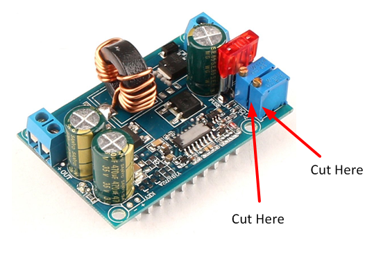
5. When the groove is deep enough, cut through the short side of the trimmer body. Don't attempt to cut through the metal adjustment screw.
6. At this point, the trimmer body will crack and separate in half. Remove the ceramic disk and brass adjustment hardware.
7. Using needle nose pliers, straighten the three wires sticking up from the remains of the trimmer body.
8. Carefully cut away the remaining bottom of the trimmer body leaving only the three wires sticking up from the PCB. Do not cut these wires as the remaining length will aid in removing the wires from the PCB.
9. Repeat steps 2 through 8 for the remaining trimmer resistor.
10. Desolder the trimmer wires and clear as much as solder as possible from the pad holes.
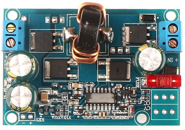
By working carefully and slowly, it is easy to remove the trimmer resistors without harming nearby components or the PCB.
11. Remove the 10A output fuse and replace with a 3A fuse.
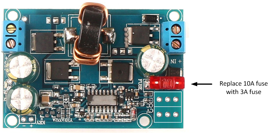
12. Cut 4" lengths of #28 or smaller stranded hookup wire. Choose wire with different color jackets to make identification easier when the wires are soldered to the potentiometers in a later step.
13. Strip 1/4" insulation from both ends of each wire and tin the ends with solder.
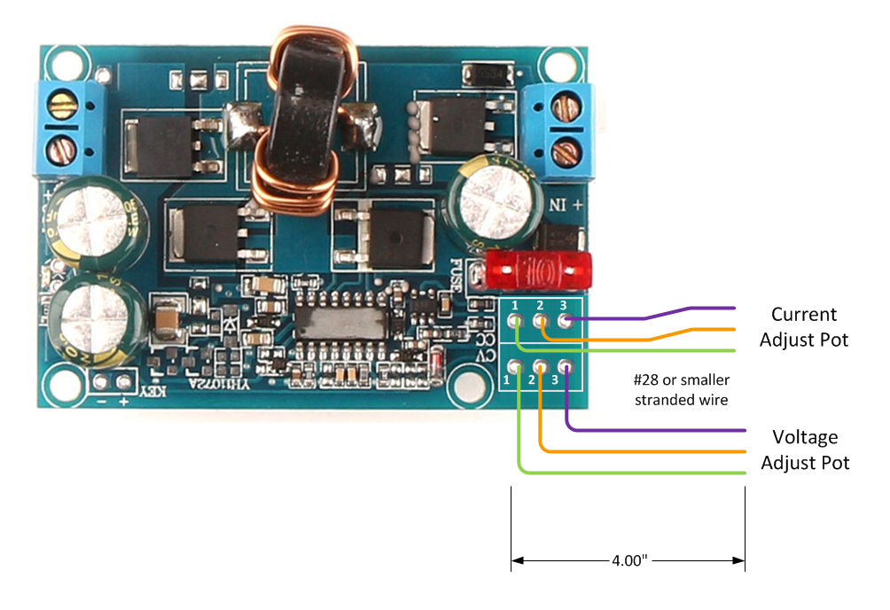
14. Solder each wire to the DC-DC converter solder pads as illustrated above.
Repeat the above steps for DC-DC Converter #2.
Note: In the illustration above the potentiometer pads are labeled 1, 2, and 3. These numbers (and wire colors) will be referred to when soldering the converter leads to the potentiometers. The jacket color chosen in this step is arbitrary. Any color can be used as long as the builder remembers to match the instructable colors with the actual colors so that the potentiometer leads are soldered to the correct pin.
Attach Enclosure Standoffs Using Screws and Insulating Washers
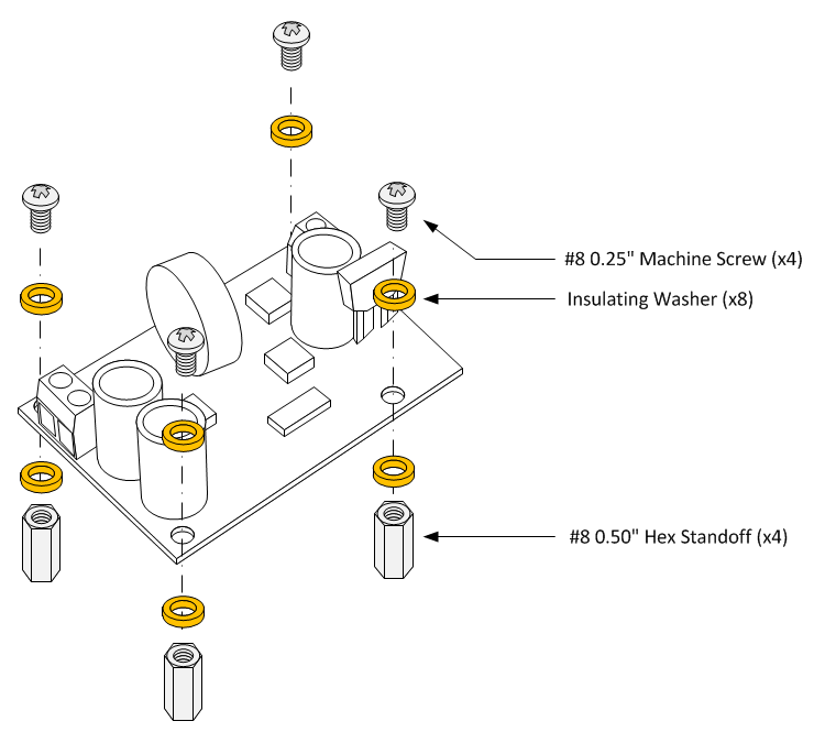
The IAASR SimCase product comes with 9 standoffs and 18 machine screws that work perfectly with the DROK DC-DC converters. Remove these standoffs from the case for use with mounting the converters.
If using a different enclosure, the converters will require eight #8 hex standoffs and 16 #8 machine screws.
Insulating washers are used ensure no exposed traces on the DC-DC converters come in contact with the enclosure and AC safety ground. They also add some height to the standoffs so that there is enough clearance for the PCB heat sink.
1. Insert one insulating washer on a #8 machine screw.
Note: The washer may be a tight fit on some screws. If the washer cannot be easily installed on the machine screw, increase the diameter of the washer slightly with a push drill.
2. Insert the machine screw and washer into a mounting hole on DC-DC converter #1.
3. Insert one insulating washer onto the screw where it exits the opposite side of the PCB.
4. Thread the hex standoff onto the screw until hand tight.
5. While holding the standoff with a pair of pliers or adjustable wrench, firmly tighten the screw.
6. Repeat steps 1 through 5 for the remaining PCB mounting holes.
Repeat the above for the DC-DC Converter #2.
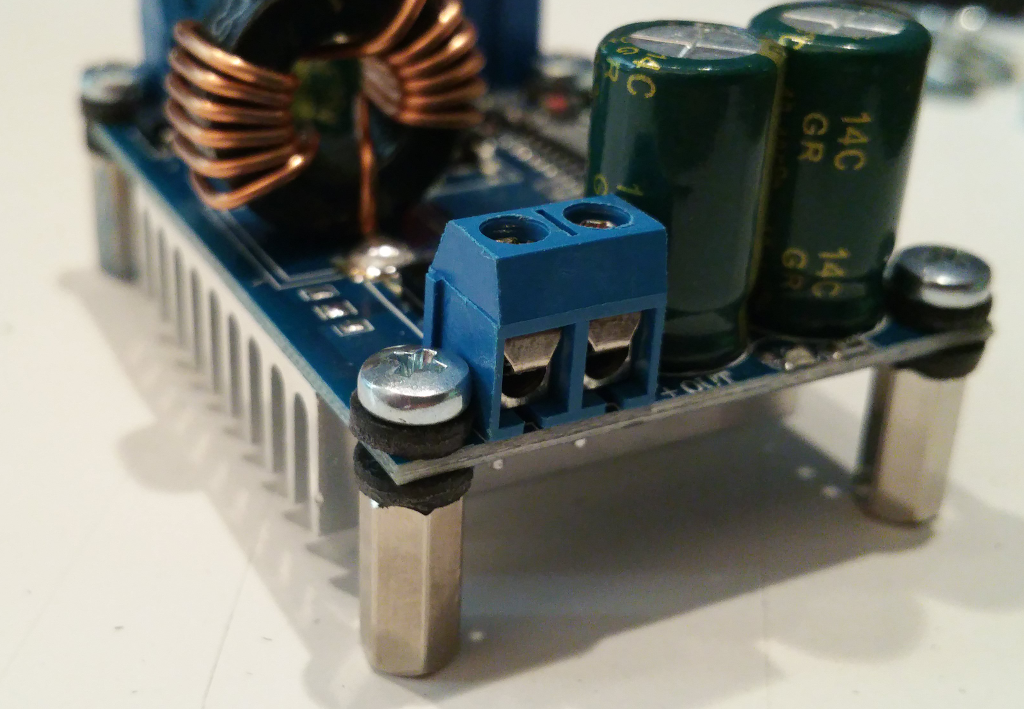
Install DC-DC Converters
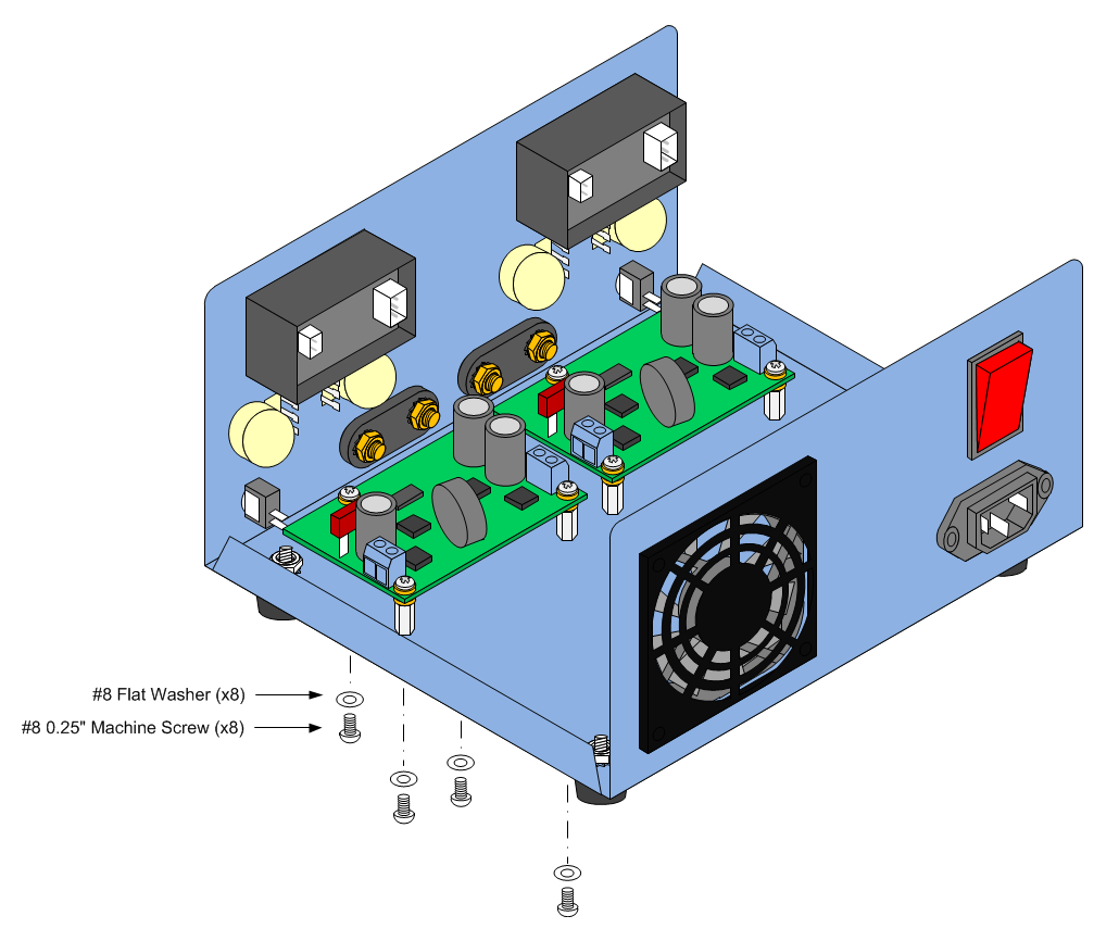
1. Line up the holes in the front of the enclosure with the hex standoffs of DC-DC Converter #1.
2. Insert a #8 flat washer onto a #8 0.5" machine screw.
3. Tread the machine screw through the bottom of the enclosure and into the hex standoff.
4. Hand tighten the machine screw.
5. Repeat steps 2 through 4 for each remaining hex standoff.
6. When all 4 machine screws and flat washers are installed, firmly tighten each screw.
7. Repeat steps 1 through 6 for DC-DC converter #2.
Build Front Panel Cables
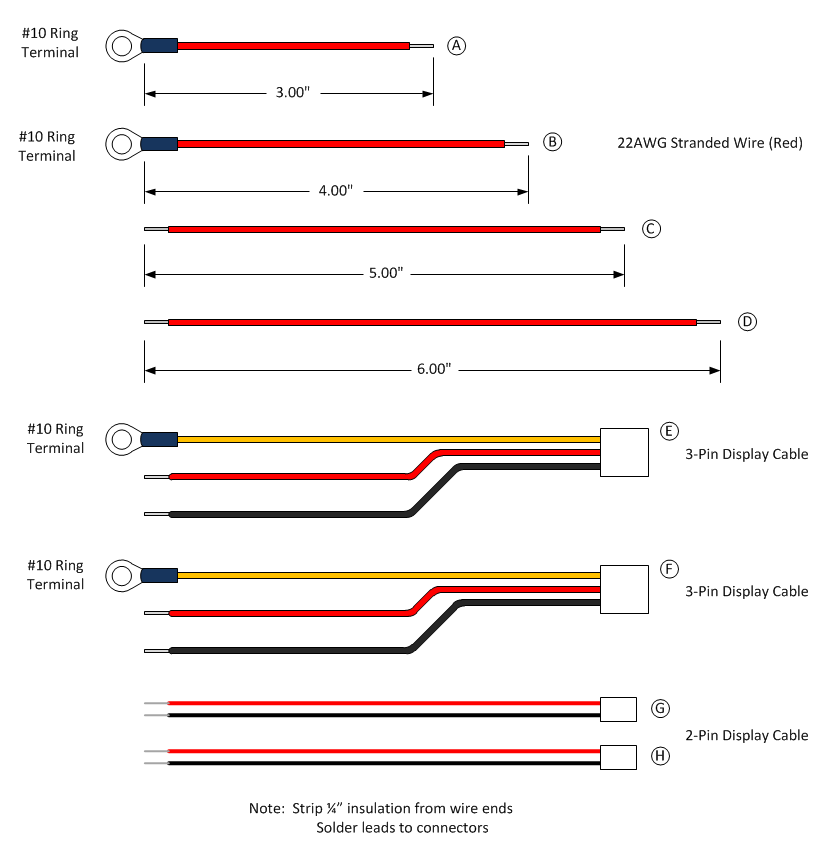
1. Cut a piece of 22AWG stranded red wire 4" long. Strip 1/4" insulation from each end and tin with solder.
2. Solder a #10 Ring Connector on one end of the 4" wire wire.
3. Cut a piece of 22AWG stranded red wire 3" long. Strip 1/4" insulation from each end and tin with solder.
4. Solder a #10 Ring Connector on one end of the 3" wire.
5. Cut a piece of 22AWG stranded red wire 5" long. Strip 1/4" insulation from each end and tin with solder.
6. Cut a piece of 22AWG stranded red wire 6" long. Strip 1/4" insulation from each end and tin with solder.
7. Strip 1/4" insulation from each lead attached to the 3-pin display connector and tin with solder.
8. Solder a #10 Ring connector to both Yellow leads attached to the 3-pin display connector.
9. Strip 1/4" insulation from each lead attached to the 2-pin display connector and tin with solder.
Wire the Front Panel Power Connections
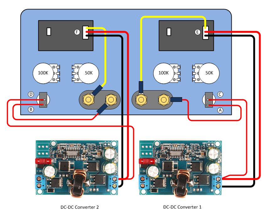
Use the diagram above in parallel with the following instructions to complete the output power connections on the front panel.
1. Remove the hex bolt and lock washer from the positive (Red) Power Supply 1 binding post.
2. Install the Ring Terminal of Cable A followed by the lock washer onto the positive (Red) Power Supply 1 binding post.
3. Thread the hex bolt onto the positive (Red) Power Supply 1 binding post and tighten firmly. Do not over-tighten the hex bolt.
4. Solder the free end of Cable A onto the lower pin of the Power Supply 1 SPST power switch.
5. Remove the hex bolt and lock washer from the positive (Red) Power Supply 2 binding post.
6. Install the Ring Terminal of Cable B followed by the lock washer onto the positive (Red) Power Supply 2 binding post.
7. Thread the hex bolt onto the positive (Red) Power Supply 2 binding post and tighten firmly. Do not over-tighten the hex bolt.
8. Solder the free end of Cable B onto the lower pin of the Power Supply 2 SPST power switch.
9. Solder one end of Cable C to the upper pin of the Power Supply 1 SPST power switch. Route the other end of Cable C to the output connector of DC-DC Converter 1 but do not attach yet.
10. Solder one end of Cable D to the upper pin of the Power Supply 2 SPST power switch. Route the other end of Cable D to the output connector of DC-DC Converter 2 but do not attach yet.
11. Remove the hex bolt and lock washer from the negative (Black) Power Supply 1 binding post.
12. Install the Ring Terminal of Cable E followed by the lock washer onto the negative (Black) Power Supply 1 binding post.
13. Thread the hex bolt onto the negative (Black) Power Supply 1 binding post and tighten firmly. Do not over-tighten the hex bolt.
14. Remove the hex bolt and lock washer from the negative (Black) Power Supply 2 binding post.
15. Install the Ring Terminal of Cable F followed by the lock washer onto the negative (Black) Power Supply 2 binding post.
16. Thread the hex bolt onto the negative (Black) Power Supply 2 binding post and tighten firmly. Do not over-tighten the hex bolt.
17. Plug the 3-pin connector of Cable E onto Power Supply 1 display module.
18. Plug the 3-pin connector of Cable F onto Power Supply 2 display module.
19. Insert the Red wire from Cable E and the Red wire Cable C into the DC-DC Converter 1 output terminal block positive (+) position and firmly tighten the terminal block screw. Do not over-tighten the terminal block screw.
20. Insert the Black wire from Cable E into the DC-DC Converter 1 output terminal block negative (-) position and firmly tighten the terminal block screw. Do not over-tighten the terminal block screw.
21. Insert the Red wire from Cable F and the Red wire Cable D into the DC-DC Converter 2 output terminal block positive (+) position and firmly tighten the terminal block screw. Do not over-tighten the terminal block screw.
22. Insert the Black wire from Cable F into the DC-DC Converter 2 output terminal block negative (-) position and firmly tighten the terminal block screw. Do not over-tighten the terminal block screw.
Wire the Front Panel Potentiometers
Use the diagrams below in parallel with the following instructions to complete the potentiometer connections on the front panel.
1. Solder the CV leads from DC-DC Converter 1 to the 50K voltage adjust potentiometer. Solder pins 1 through 3 on the DC-DC Converter PCB to pins 1 through 3 on the potentiometer as illustrated below.
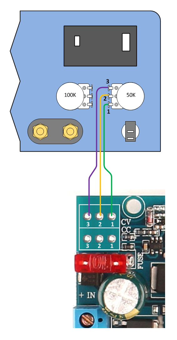
2. Solder the CC leads from DC-DC Converter 1 to the 100K current adjust potentiometer. Solder pins 1 through 3 on the DC-DC Converter PCB to pins 1 through 3 on the potentiometer as illustrated below.
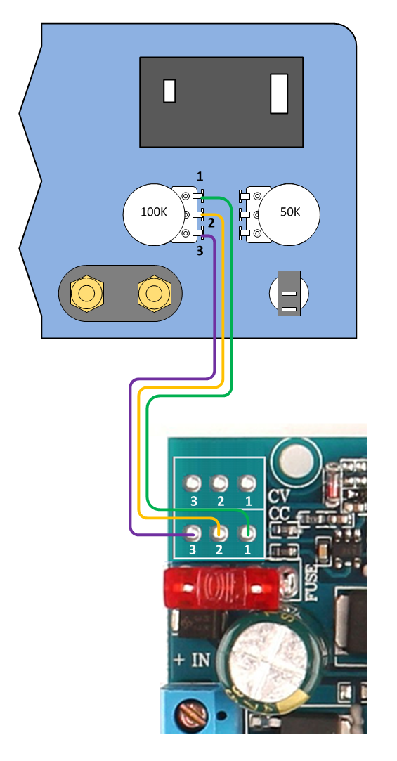
3. Solder the CV leads from DC-DC Converter 2 to the 50K voltage adjust potentiometer. Solder pins 1 through 3 on the DC-DC Converter PCB to pins 1 through 3 on the potentiometer as illustrated below.
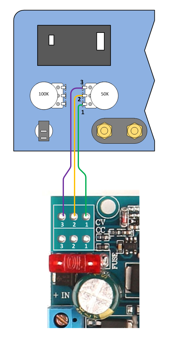
4. Solder the CC leads from DC-DC Converter 2 to the 100K current adjust potentiometer. Solder pins 1 through 3 on the DC-DC Converter PCB to pins 1 through 3 on the potentiometer as illustrated below.
Dress Front Panel Wiring With Plastic Cable Ties
Double-check front panel wiring. Using small plastic cable ties, dress the front panel cabling for appearance.
Wire the 24V Power Supplies
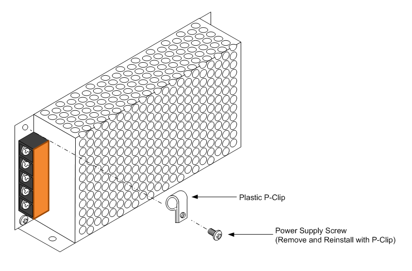
1. Remove one screw above the barrier strip from each 24V power supply as indicated in the above illustration.
2. Install a plastic P-Clip using the screw just removed oriented as indicated in the above diagram.
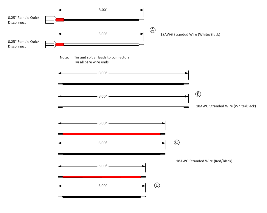
3. Build cables A, B, C, and D as indicated in the diagram above. Strip 1/4" insulation from both ends of each wire. Solder all connectors and tin all bare wire ends.
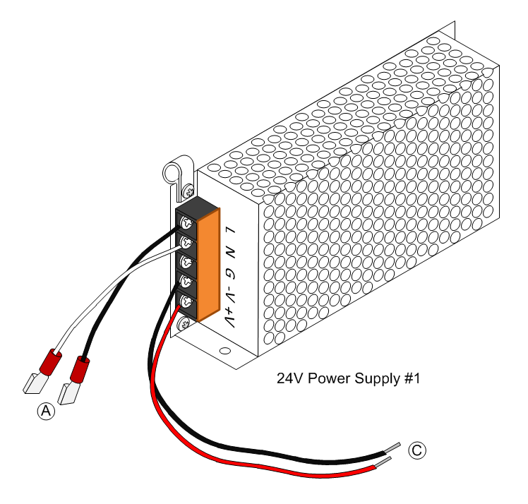
4. Attach cables A and C to 24V Power Supply 1 as indicated in the above illustration. The Black wire of cable A connects to the barrier screw marked 'L'. The White wire of cable A connects to the barrier screw marked 'N'. The Black wire of cable C connects to the barrier screw marked '-V'. The Red wire of cable C connects to the barrier screw marked '+V'.
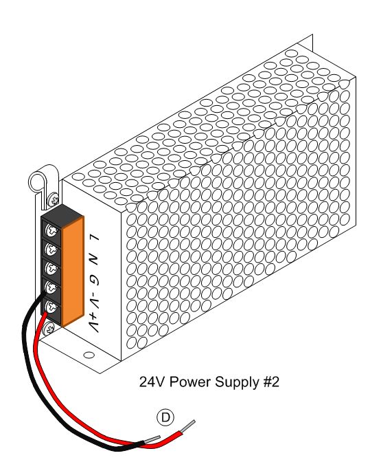
5. Attach cable D to 24V Power Supply 2 as indicated in the above illustration. The Black wire of cable D connects to the barrier screw marked '-V'. The Red wire of cable D connects to the barrier screw marked '+V'.
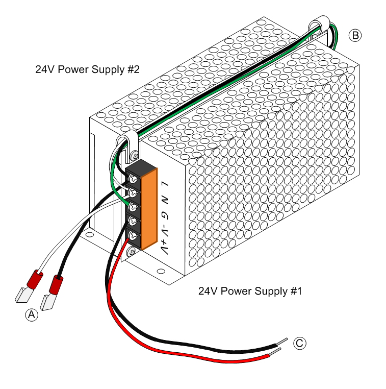
6. Place 24V Power Supply 1 and 2 back to back as illustrated in the diagram above.
7. Connect cable B between 24V Power Supply 1 and 2 by threading the wire through the P-Clips. The Black wire of cable B connects to the barrier screw marked 'L' on both supplies. The White wire of cable B connects to the barrier screw marked 'N' on both supplies. The Green wire of cable B connects to the barrier screw marked 'G' on both supplies.
Install the 24V Power Supplies
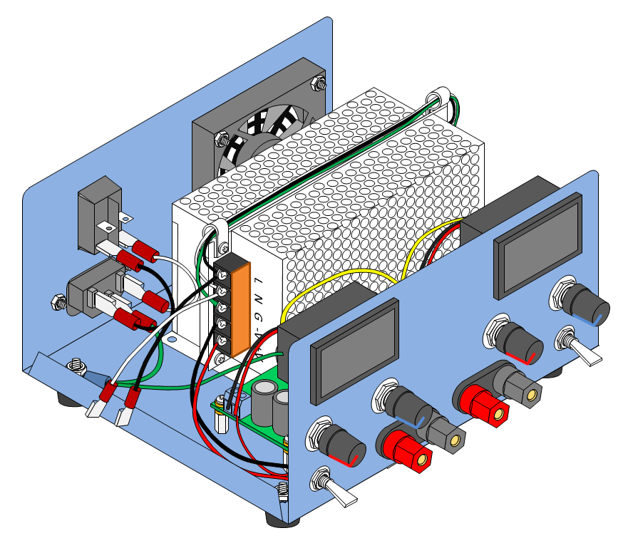
Lift both 24V Power Supplies and place them in the enclosure as indicated in the diagram above. Verify that the power supply modules align with the enclosure mounting holes but do not fasten the power supplies at this time.
Complete Wiring of the 24V Power Supplies
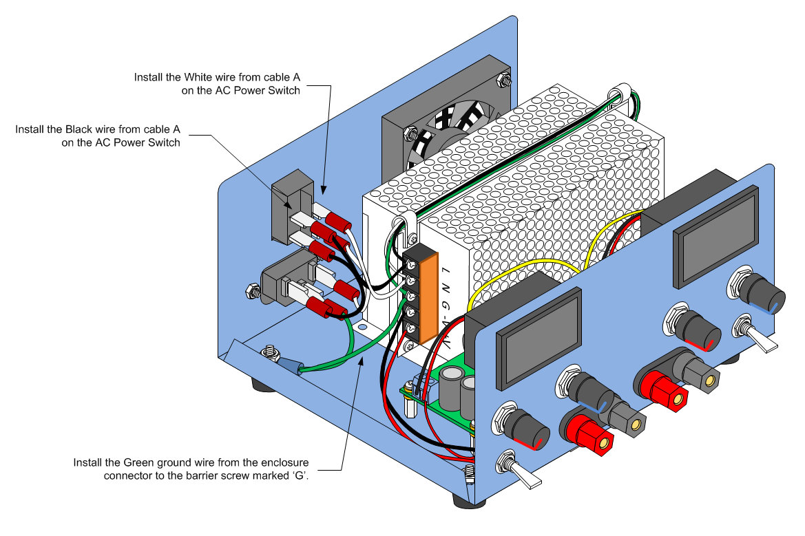
1. Attach the 24V Power Supply AC input and ground leads as indicated in the diagram above above.
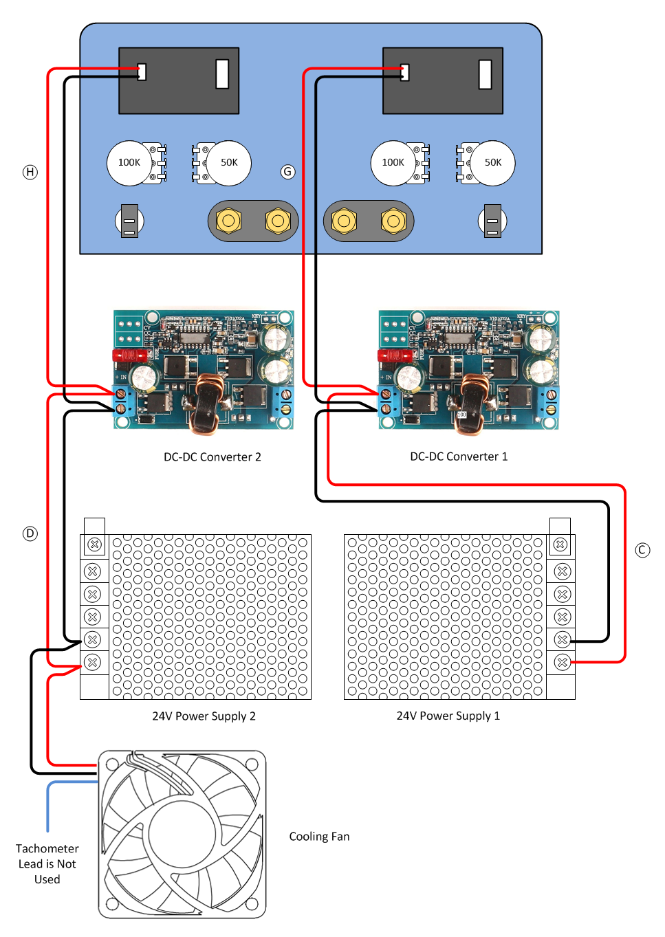
2. Plug the 2-Pin connectors G and H into the V/I displays.
3. Connect cable C from 24V Power Supply 1 to DC-DC Converter 1. The Red wire connects to the 'IN+' screw terminal of the DC-DC Converter as shown in the diagram above. The Black wire connects to the 'IN-' screw terminal of the DC-DC Converter as shown in the diagram above.
4. Connect 2-Pin cable G to DC-DC Converter 1. The Red wire connects to the 'IN+' screw terminal of the DC-DC Converter as shown in the diagram above. The Black wire connects to the 'IN-' screw terminal of the DC-DC Converter as shown in the diagram above.
5. Connect cable D from 24V Power Supply 2 to DC-DC Converter 2. The Red wire connects to the 'IN+' screw terminal of the DC-DC Converter as shown in the diagram above. The Black wire connects to the 'IN-' screw terminal of the DC-DC Converter as shown in the diagram above.
6. Connect 2-Pin cable H to DC-DC Converter 2. The Red wire connects to the 'IN+' screw terminal of the DC-DC Converter as shown in the diagram above. The Black wire connects to the 'IN-' screw terminal of the DC-DC Converter as shown in the diagram above.
7. Connect the Cooling Fan cable to 24V Power Supply 2 as shown in the diagram above. The Red wire connects to the barrier screw marked '+V' on 24V Power Supply 2. The Black wire connects to the '-V' barrier screw on 24V Power Supply 2. The Cooling Fan Blue tachometer wire is not used.
8. Secure the 24V power supplies to the enclosure with four #8 machine screws, washers, and lock nuts.
9. Dress all wires and secure with cable ties.
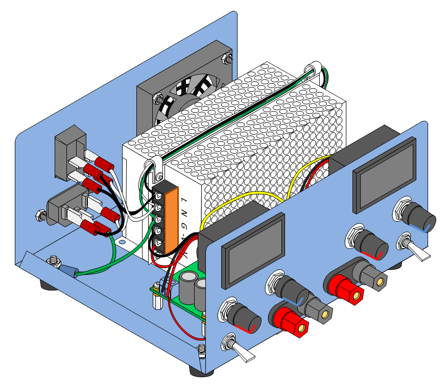
Testing Before Power-On
Before plugging in and powering on the completed power supply for the first time, perform the following checks:
1. Using a digital VOM set to Ohms, measure the resistance between the 'L' and 'N' binding screws on 24V Power Supply 1. The VOM should read very high (>10K Ohms) or infinite resistance. If the VOM reads low resistance or a short circuit, verify that all AC wiring is correct using the power supply schematic diagram. DO NOT CONNECT THE POWER SUPPLY TO AN AC OUTLET UNTIL THE MEASUREMENT IS CORRECT (VERY HIGH OR INFINITE RESISTANCE).
2. Using a digital VOM set to OHMS, measure the resistance between the 'L' and 'G' binding screws on 24V Power Supply 1. The VOM should read very high (>10K Ohms) or infinite resistance. If the VOM reads low resistance or a short circuit, verify that all AC wiring is correct using the power supply schematic diagram. DO NOT CONNECT THE POWER SUPPLY TO AN AC OUTLET UNTIL THE MEASUREMENT IS CORRECT (VERY HIGH OR INFINITE RESISTANCE).
3. Using a digital VOM set to OHMS, measure the resistance between the 'N' and 'G' binding screws on 24V Power Supply 1. The VOM should read very high (>10K Ohms) or infinite resistance. If the VOM reads low resistance or a short circuit, verify that all AC wiring is correct using the power supply schematic diagram. DO NOT CONNECT THE POWER SUPPLY TO AN AC OUTLET UNTIL THE MEASUREMENT IS CORRECT (VERY HIGH OR INFINITE RESISTANCE).
If any of the above measurements are not correct and all wiring has been verified, do not proceed and do not connect the power supply to an AC outlet. Contact the 24V AC Power Supply representative for further instructions.
4. Make sure the power supply output SPST switches are in the OFF (Down) position.
5. Using a digital VOM set to OHMS, measure the resistance between the Positive (Red) output binding post and the Negative (Black) output binding post of power supply 1 (Left Side). The VOM should read very high (>10K Ohms) or infinite resistance. If the VOM reads low resistance or a short circuit, verify that all DC-DC Converter output wiring is correct using the power supply schematic diagram. Check that the output binding post is properly seated in the front panel and that there are no bits of wire or solder touching the power supply enclosure or other circuit connections. Do not proceed until the resistance is within the indicated range (>10K Ohms).
6. Using a digital VOM set to OHMS, measure the resistance between the Positive (Red) output binding post and the Negative (Black) output binding post of power supply 2 (Right Side) . The VOM should read very high (>10K Ohms) or infinite resistance. If the VOM reads low resistance or a short circuit, verify that all DC-DC Converter output wiring is correct using the power supply schematic diagram. Check that the output binding post is properly seated in the front panel and that there are no bits of wire or solder touching the power supply enclosure or other circuit connections. Do not proceed until the resistance is within the indicated range (>10K Ohms).
7. Put both power supply output SPST switches in the ON (Up) position.
8. Using a digital VOM set to OHMS, measure the resistance between the Positive (Red) output binding post and the Negative (Black) output binding post of power supply 1 (Left Side). The VOM should read very high (>10K Ohms) or infinite resistance. If the VOM reads low resistance or a short circuit, verify that all DC-DC Converter output wiring is correct using the power supply schematic diagram. If after verifying that circuit wiring is correct, do not proceed. Contact the DC-DC Converter representative for further instructions.
9. Using a digital VOM set to OHMS, measure the resistance between the Positive (Red) output binding post and the Negative (Black) output binding post of power supply 2 (Right Side). The VOM should read very high (>10K Ohms) or infinite resistance. If the VOM reads low resistance or a short circuit, verify that all DC-DC Converter output wiring is correct using the power supply schematic diagram. If after verifying that circuit wiring is correct, do not proceed. Contact the DC-DC Converter representative for further instructions.
10. Attach a power cord to the power supply AC Input Module. DO NOT PLUG THE POWER CORD INTO AN AC OUTLET.
11. Turn on the AC Power Switch.
12. Using a digital VOM set to OHMS, measure the resistance between the power cord hot and neutral conductors. The VOM should read very high (>10K Ohms) or infinite resistance. If the VOM reads low resistance or a short circuit, verify that all AC wiring between the AC Input Module and the AC Power Switch is correct using the power supply schematic diagram. DO NOT CONNECT THE POWER SUPPLY TO AN AC OUTLET UNTIL THE MEASUREMENT IS CORRECT (VERY HIGH OR INFINITE RESISTANCE).
13. Using a digital VOM set to OHMS, measure the resistance between the power cord hot and ground conductors. The VOM should read very high (>10K Ohms) or infinite resistance. If the VOM reads low resistance or a short circuit, verify that all AC wiring between the AC Input Module and the AC Power Switch is correct using the power supply schematic diagram. DO NOT CONNECT THE POWER SUPPLY TO AN AC OUTLET UNTIL THE MEASUREMENT IS CORRECT (VERY HIGH OR INFINITE RESISTANCE).
14. Using a digital VOM set to OHMS, measure the resistance between the power cord neutral and ground conductors. The VOM should read very high (>10K Ohms) or infinite resistance. If the VOM reads low resistance or a short circuit, verify that all AC wiring between the AC Input Module and the AC Power Switch is correct using the power supply schematic diagram. DO NOT CONNECT THE POWER SUPPLY TO AN AC OUTLET UNTIL THE MEASUREMENT IS CORRECT (VERY HIGH OR INFINITE RESISTANCE).
Attach the Top Cover
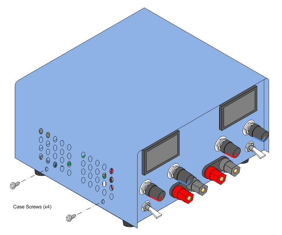
Place the enclosure top over the power supply chassis and line up the holes in the top cover with the holes in the base. Secure the top to the base with the screws supplied by the enclosure vendor.
Power-On Testing
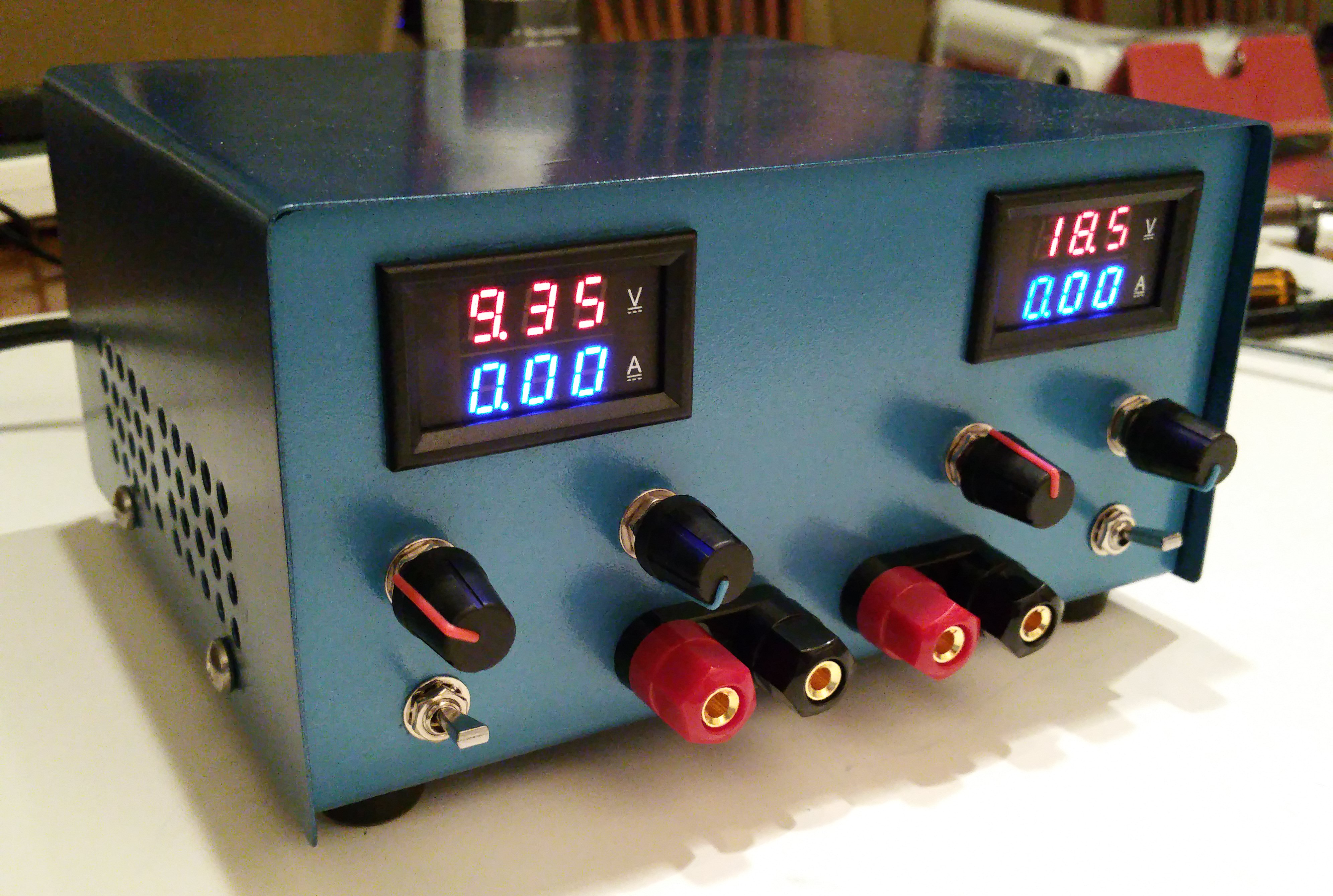
1. Verify that the back panel AC Power Switch is in the Off position.
2. Verify that the front panel Output SPST switches are in the Off (Down) position.
3. Verify that the front panel Voltage and Current controls are rotated fully counter clockwise.
3. Plug the power supply power cord into an AC outlet.
4. Turn on the AC Power Switch
The AC Power Switch will illuminate. If it does not illuminate, verify that the AC Outlet is energized and that the power cord is fully plugged into the outlets at both ends. IF THE AC POWER SWITCH DOES NOT ILLUMINATE, REMOVE THE POWER CORD FROM THE AC OUTLET.
5. The Cooling Fan will turn on and the front panel V/I displays will illuminate. If the cooling fan or V/I displays do not come on, turn off the AC power switch and disconnect the power cord from the AC outlet. Remove the top cover and verify that the fan or display wiring is correct. If the fan or display wiring is correct, contact the fan or display representative for further instructions.
6. The front panel V/I displays should indicate approximately 1.00V and 1.50V for the output voltage and 0.00A for the output current. If the V/I display indicates approximately 20V with the voltage controls fully counter-clockwise, turn off the AC power switch and disconnect the power cord from the AC outlet. Remove the top cover and verify that the voltage potentiometer wiring is correct. If the potentiometer wiring is correct, contact the DC-DC Converter representative for further instructions.
7. Rotate the Power Supply 1 (Left Side) voltage control clockwise. The V/I display should show the output voltage increasing as the control is turned clockwise and decreasing when the control is turned counter-clockwise. If the V/I display does not change in value as the voltage control is rotated, turn off the AC power switch and disconnect the power cord from the AC outlet. Remove the top cover and verify that the voltage potentiometer wiring is correct. If the potentiometer wiring is correct, contact the DC-DC Converter representative for further instructions.
8. Rotate the Power Supply 2 (Right Side) voltage control clockwise. The V/I display should show the output voltage increasing as the control is turned clockwise and decreasing when the control is turned counter-clockwise. If the V/I display does not change in value as the voltage control is rotated, turn off the AC power switch and disconnect the power cord from the AC outlet. Remove the top cover and verify that the voltage potentiometer wiring is correct. If the potentiometer wiring is correct, contact the DC-DC Converter representative for further instructions.
Optional Load Testing
9. Rotate all front panel voltage and current controls fully counter clockwise.
10. Verify that both output SPST switches are in the Off (Down) position.
10. Attach a 10 Ohm, 20W resistor between the Positive (Red) and Negative (Black) output binding posts of Power Supply 1 (Left Side).
11. Flip the Power Supply 1 output SPST switch to the ON position.
12. The V/I display should show an output current of approximately 0.10A
13. Flip the Power Supply 1 output SPST switch to the OFF position.
14. Rotate the voltage control until the V/I display reads 10V.
15. Flip the Power Supply 1 output SPST switch to the ON position.
16. The V/I display should indicate a reduced output voltage and between 0.10A and 0.20A.
17. Slowly rotate the current control until the V/I display reads 10V and approximately 1.00A.
18. Flip the Power Supply 1 output SPST power switch to the OFF position.
19. Remove the 10 Ohm, 20W resistor from the output binding post of Power Supply 1.
20. Attach a 10 Ohm, 20W resistor between the Positive (Red) and Negative (Black) output binding posts of Power Supply 2 (Right Side).
21. Repeat steps 11 through 19 for Power Supply 2.
22. Turn off the AC Power Switch and disconnect the AC Power Cord from the AC wall outlet.
The Dual Switched-Mode Power Supply is ready for use.
One Tube AM Radio
I've been fascinated with the early history of radio and television between 1870 through 1929 since reading a very old copy of "The Boys Second Book of Radio and Electronics" by Alfred Morgan, found in the dusty science shelves of my highschool library (I'm a "geek" and that book made me happy). This period is dominated by some very interesting and bizarre personalities like Thomas Edison, Guglielmo Marconi, John Fleming, Nikola Tesla, Reginald Fessenden, Lee de Forest, and Edwin Armstrong. These people are credited with the fundamental inventions commercialized by RCA, GE, AT&T, and Westinghouse; companies which flourished in the golden age of radio and still exist today!
They were mostly experimenters and tinkerers at a time when academic research was often unconcerned with the practical application of a scientific discovery. As a result the industry did not have a good understanding of how the electronic devices they were building actually worked. At times the money to be made from broadcast radio, the competitive litigation that inevitably follows the profits, and the government regulation intended to control on overheated emerging industry became more significant than the technology. Kind of like it does today, right? These are the major reasons why there isn't a Wright Brothers airplane company around today.
The development of radio even struggled through two world wars and the Great Depression. But consumer desire for a well-deserved break from daily life through entertainment created demand for innovation in radio that sustained the industry beyond hard times. Just like it does today. This is what I find inspiring from all that I have learned from engineering: Imperfect people with mostly good intentions and sometimes bad behavior, equipped with what the future will refer to as "stone knives and bearskins", can still accomplish something good and useful for society. When I see that I think, "There's hope for us all".
The 60's and 70's were the golden age of electronic kit building. The novice had a great many educational kits to choose from that taught basic skills and electronics theory while assembling a device that could do something useful or entertaining. An advanced builder could use "sweat equity" to inexpensively obtain popular electronic products like HiFi stereo systems, color televisions, CB radios, and automotive test equipment.
Today there are still quite a few electronics kits available for education purposes, but rapidly evolving features and shrinking components ended the consumer electronics kit business. I would have loved to have assembled some of the products that were popular in the 70's, but unfortunately most of the companies that made all those wonderful kits were gone when I began my career. In honor of a great set of educational Radio Shack electronics project kits available during the 60's and 70's, I've redesigned the original Science Fair brand One Tube AM Radio (Catalog #28-100) using modern components still available from electronics component re-sellers in the US. All of the components in the updated kit can be found on Amazon.
There were many things Radio Shack did extremely well during its prime. It's too bad the company is "history" along with Lafayette Radio, Allied Radio, Heathkit, Popular Electronics, Byte, and many others who were here for a time and are here no more. Their humor, their creativity, hand-drawn artwork... Experimenters young and old, especially in rural areas, are less served by their demise.
For the nostalgic or the enthusiast who would like to build an updated version of this classic radio, I've included schematics, parts information, assembly documentation, and pictures of a completed and tested One Tube AM Radio based on the original from 1968, which is itself derived from a design attributed to Lee de Forest in 1908. If like me you enjoy walking in the footsteps of the great inventors of the 20th century, you'll love this project.
Just a Song Before I Go...
An original Radio Shack One Tube AM Radio kit was given to me by a mentor of mine when I was still learning how to solder. But I didn't really have the proper tools for electronics assembly work. While putting the kit together, I accidentally broke off one of the tube socket pins. I tried as hard as I could to solder a wire to the little stub of metal sticking out but couldn't. When I went to my local Radio Shack, the One Tube Am Radio kit had been long discontinued. "A 7-pin tube socket? Ha! Good luck kid." So I shelved the kit and moved on. But I never forgot that early failure. So for me this project was a redemption, so to speak.
After redesigning the tuning circuit with available parts and building the radio, I was disappointed in its performance. After checking with a few people online that could remember building the original Radio Shack kit back when it was available, I found the consensus to be that the radio never really worked well. Slightly better than a crystal radio I believe was the usual outcome. I didn't want a nice looking tube radio that didn't work, so I decided to rewire it using some old amateur radio articles published in the 1920's for inspiration. I was very happy to find that the new design presented in this article worked much better than the original. I can easily receive all three local AM stations in my city with a 10ft piece of wire for an antenna and an earth ground connection.
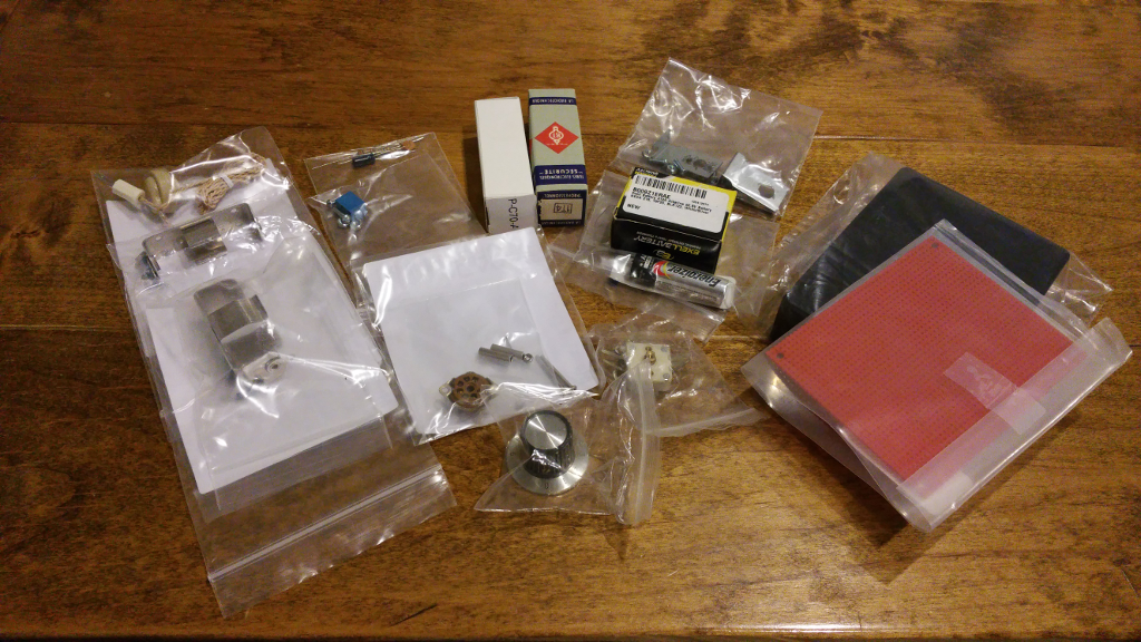
Although I feel my results made the project costs, time, and effort worthwhile I think it wise to present to the reader a few observations and opinions:
1. I recommend this project for the intermediate to expert builder. Moderate soldering skills are required and some metal fabrication must be done for the variable capacitor and tuning coil brackets. Connecting and soldering wires to the mounted tube socket can be a challenge for the inexperienced. Several of the components are fragile and relatively expensive. If you have successfully completed a few projects from scratch using breadboard construction techniques, then you should be good to go for the One Tube AM Radio project.
2. If you decide to build this project, you should have no problem obtaining the parts. I deliberately avoided using rare or hard to find vintage parts in order to save those for the folks that are trying to restore a vintage radio. Instead, I provide component names and part numbers from distributors of new or new-old-stock in volume that are compatible with the original look of the radio as much as possible.
3. The 22.5 V battery I used is the most expensive component of the lot at $25. I chose that battery because I wanted to keep to the original look and feel as much as possible, which required me to spend more money than I would otherwise recommend. By all means feel free to substitute three 9V batteries in series for the 22.5V battery.
Should you decide to use the 22.5V battery I did, you can obtain it from Excell via Amazon (ASIN B009Z1ERAE). This battery works extremely well in the radio, and will run for 4 months of continuous use or more than a year of occasional use. I suspect what Excell has done is connect fifteen 180mAh alkaline button cells in series and secure them to a plastic carrier that is the same size as the old NEDA 215. So perhaps there is some hacking that can be done instead of buying a new one.
4. Current consumption on the 22.5V B Battery is 40uA so it can run quite a long time. However, A Battery consumption on the 1T4 tube is 50mA, in line with the manufacturers specifications. Which means you can expect between one to two days of continuous use and perhaps several weeks of occasional use. Keep a pack of AA's handy.
5. The most significant deviation from the original Radio Shack kit is the use of a tuning capacitor. After many days spent searching through the web for a volume source for the antenna coil, I concluded that it is not possible to obtain one similar to the original without resorting to a rare vintage supplier. So I decided to use an adjustable Miller-style antenna coil from AmplifiedParts.com and tuning capacitor from uxcell.com. The adjustable ferrite slug in the antenna coil I used allows for alignment of the tuning range only. Main tuning is provided by the variable capacitor. But the tuning coil does look enough like the original part to make me happy, and the redesign allows the radio to tune into the Extended AM Broadcast band between 1610 kHz and 1710 kHz, something the original kit wasn't designed to do.
6. This project requires "alignment" in order to set the tuning range between 540 kHz and 1710 kHz. Which means the builder will need a hex alignment tool for the tuning coil. I used a 0.100" hex alignment tool from Aven Tools (Amazon ASIN B001Q4YGQS) which is a nice sturdy kit that has worked well for me. Alignment is best accomplished by setting the coil slug and variable capacitor trimmers as indicated in the "Before You Begin" section. An LCR meter is suggested for the most accurate alignment but is not required.
If you are still with me after all of the above, then let's get started.
Please Note: I have no business relationship with any vendors mentioned in this article. Nothing of financial value was exchanged for any recommendation I make. None of the vendors mentioned in this article provided compensation of any kind during the creation of this project. I will not be compensated in any way if you choose to build this project or purchase components from any vendor I recommend. I simply had a good experience with the vendors I recommend and believe you will too.
Obtain Components Listed in the Assembly Manual Parts List
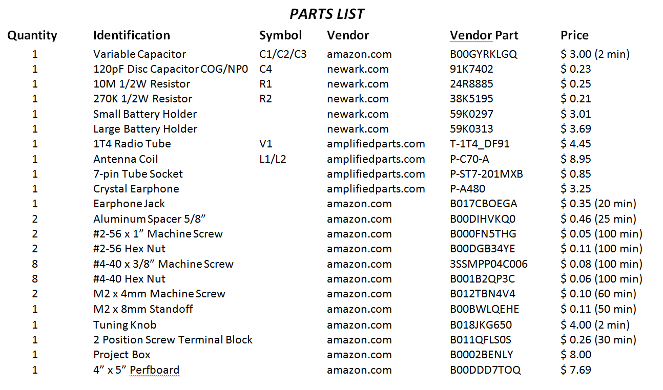
Review the parts list and obtain the components indicated. Everything but a few pieces of hardware are available on Amazon or can be obtained directly from the suppliers indicated at the bottom of the parts list.
Below are a few notes regarding the parts used for the radio:

1. Amplified Parts (www.amplifiedparts.com) is my go-to resource for tons of components used in vacuum tube amplifier and radio circuits. Tubes, knobs, jacks, coils, earphones, resistors, capacitors.. it's all there. They have tons of NOS components in regular inventory, online ordering is easy, and shipping is extremely fast. The critical components of the One Tube AM Radio were all obtained here. I purchased several 1T4 tubes, 7-pin sockets, antenna coils, and crystal earphones from AmplifiedParts and they all work great. The crystal earphone comes with a 1/8" mono phone plug so I added a 1/8" mono phone jack from Amazon. If you like to build, repair, or restore vintage equipment you have to check out Amplified Parts.
2. For bulk resistors used in project building and experimentation, I highly recommend the excellent Joe Knows Electronics (www.joeknowselectronics.com) resistor kit in 1/4W and 1/2W sizes. These kits include the most popular values you will be likely to use with 1% tolerance (which is overkill for basic circuits but nice to have). NOTE: As of 2026, Joe Knows Electronics is no longer in business. I have left the content here for historical purposes. There are many resistor assortments available on Amazon at great prices.
3. I strongly recommend ordering NP0 ceramic disk capacitors from Allied, Mouser or Digikey as they will far outperform most anything you can get on Amazon. The Joe Knows Electronics capacitor kit is an extremely good buy for general purpose capacitors at 645 pieces for $13.00.
4. The variable capacitor (and a lot of other rather old and interesting electronic parts) can be found at Uxcell (www.uxcell.com) which seems an unlikely domain for radio stuff, but they do have a lot of radio stuff that's interesting. I've created a diagram of the variable capacitor below that will help you figure out how to wire it into radios circuits of your own design.
5. The case for the radio I built is a Hammond 1591GSBK ABS Project Box from Amazon.com with a piece of vector breadboard cut to fit on the top and spray painted with high temperature automotive flat red and finished with a semi-gloss clearcoat. I like the look of red on black, and the red color of the breadboard matched the red color of the original pbox kit. It's completely up to you how you want to house and color the kit you build.
6. The knob I used is a Radio Shack product I've had in inventory for decades. Use anything you think is cool that will fit on the varicap shaft. The shaft on the varicap is only about 1/4" long so you will need something to extend it. I used a nylon hex standoff and shaved it down to fit. Use anything you have that gives the knob a confident solid feel.
7. For those curious about the 1T4 vacuum tube, I've included the datasheet I used with the 1T4 from Amplified Parts. The evaluation I did on filament current, plate and grid current/voltage, and Mu parameters for the tube sold to me matches very closely with the parameters in the datasheet. Very useful when doing your own designs.
8. Also below is the datasheet for the antenna coil from Amplified Parts. My measurements show the following:
Primary (Pins 3/4) - 2120uH to 3372uH variable when ferrite is positioned on the primary
Secondary (Pins 1/2) - 163uH to 333uH variable when ferrite is positioned on the primary
Unloaded resonant Q is around 250.
These are the parameters I used to redesign the tuning section of the radio and they were dead on as built.
The datasheet for the 1T4 Tube is >>> HERE <<<.
The datasheet for the Tuning Capacitor is >>> HERE <<<.
The datasheet for the Tuning Coil is >>> HERE <<<.
Before You Begin - Variable Capacitor Alignment
Before you start the build process, the variable capacitor needs to be set to its minimum value by adjusting the position of the trimmer capacitors on the back. If you look closely at the back of the variable capacitor, you will notice 4 small adjustment screws.
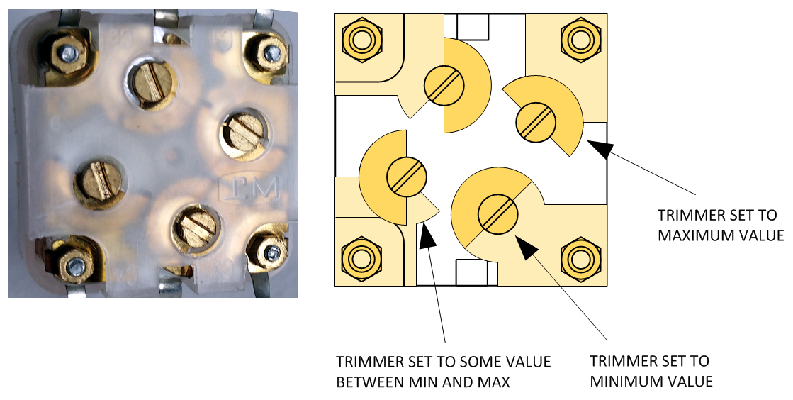
Illustration 1 - Variable Capacitor Trimmer Adjustments
These adjustment screws are provided to fine-tune the range of each section of the variable capacitor. The variable capacitor you will receive may have its trimmers set to minimum, maximum, or some value in between (See Illustration 1). What you need to do is adjust each trimmer to it's minimum value as shown in Illustration 6:
Caution: Avoid applying heavy pressure into the trimmer while turning. If the trimmer is hard to turn in one direction, try to rotate it in the opposite direction. Let the tool do the work.
1. Hold the variable capacitor with the trimmer screws facing you. Using a small precision screwdriver or the steel slotted alignment tool from the Aven kit described earlier, turn the T1 trimmer screw clock-wise or counter-clockwise as shown in Illustration 2 until it is in the position indicated in Illustration 3.
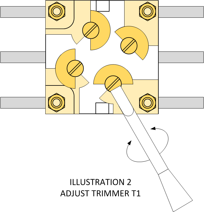
2. Do the same for trimmer T2 (see Illustration 3) until it is in the position indicated in Illustration 4.
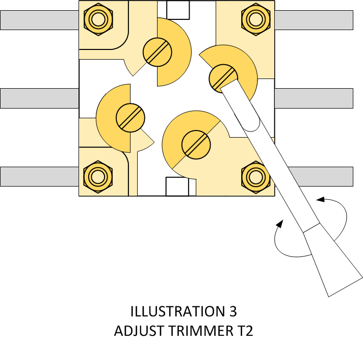
3. Do the same for trimmer T3 (see Illustration 4) until it is in the position indicated in Illustration 5.
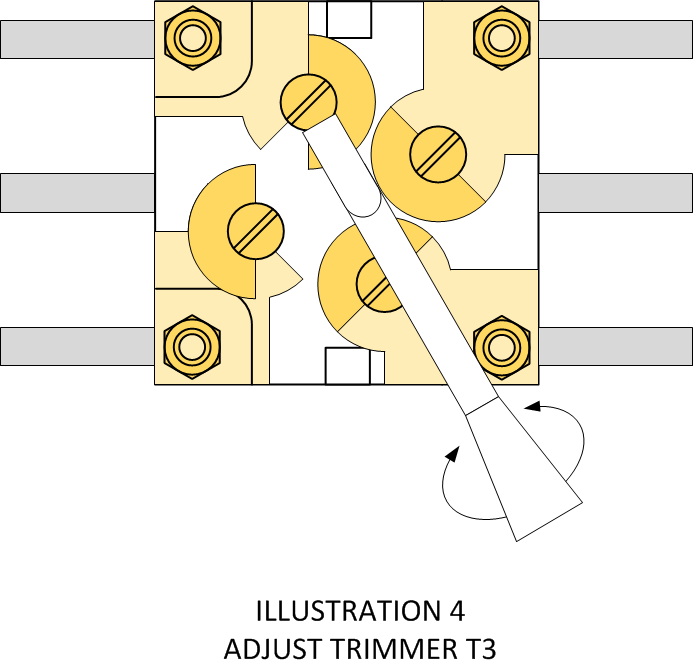
4. Do the same for trimmer T4 (see Illustration 5) and then verify that all trimmers are in their minimum value position as indicated in Illustration 6.
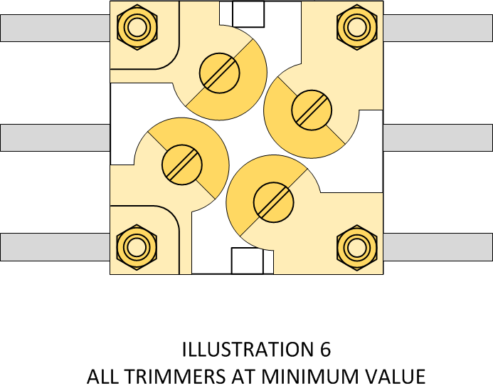
The variable capacitor is now ready for use.
If you have an LCR meter, the variable capacitor should provide the following range:
Low Value: 18pf to 24pF
High Value: 298pF to 304pF
A document describing the variable capacitor connections is included >>> HERE <<<.
Before You Begin - Antenna Coil Alignment
The P-C70-A antenna coil provides an adjustable ferrite core for fine tuning the inductance of the secondary winding so that the tuning range of the variable capacitor fits comfortably within the AM broadcast band (540 kHz to 1710 kHz). The antenna coil you will receive has not been aligned and requires adjustment before installation. The alignment can be fine tuned after installation. To align the antenna coil, follow the steps below:
Caution: Use only a 0.100" plastic hex alignment tool. A tool of the wrong size will damage the ferrite slug making it impossible to align the antenna coil. Use only the minimum force necessary to rotate the slug. Do not push against the slug while turning. Let the alignment tool do the work. Check the slug position after the first few turns to make sure it is moving in the correct direction (toward the front of the coil). If it isn't, reverse the direction of alignment tool rotation.
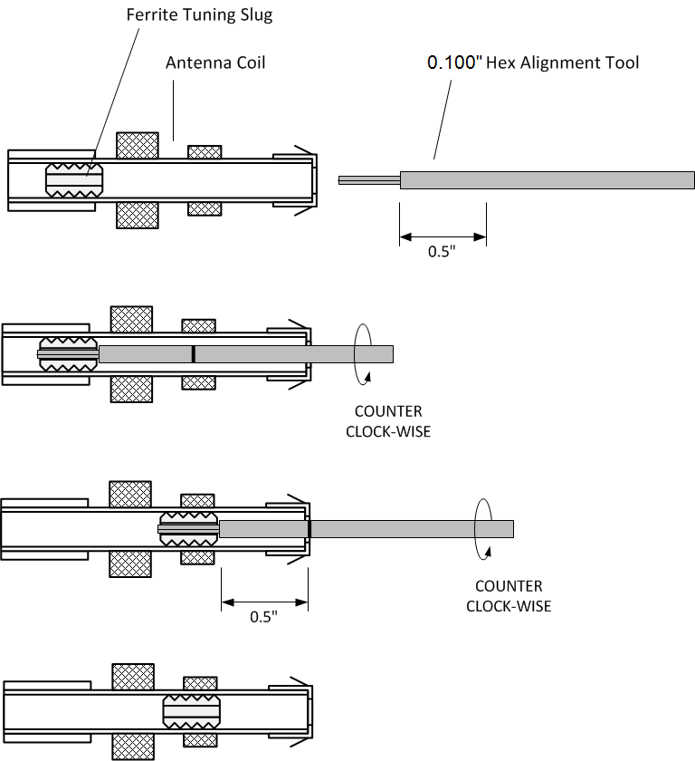
1. Measure 1/2" along the barrel of a 0.100" Hex Alignment Tool starting from the shoulder as shown in the illustration above.
2. Insert the alignment tool into the front of the antenna coil as shown until the alignment tool is fully seated into the ferrite core.
3. Rotate the alignment tool in a counter clockwise direction making sure that the alignment tool is moving out of the front of the coil instead of inward toward the back of the coil.
4. Stop rotation and remove the alignment tool when the top of the ferrite core is 1/2" from the front of the antenna coil.
The antenna coil is ready for use.
If you have an LCR meter, the coil inductance should be between 300uH and 330uH.
A datasheet for the antenna coil is included >>> HERE <<<.
Before You Begin - Fabricate Mounting Brackets
I've included templates for fabricating the mounting brackets used with the variable capacitor and the antenna coil. I used two PC card slot blanks I had laying around and simply cut them to size, drilled holes, and used a Dremel tool to grind off the flash. You can use any soft metal you have in your junk box. Or even a piece of plastic that is shaped like an 'L' bracket will work. Imagination will pay off in this step.
Caution: Always wear eye protection when using power tools. This project is more fun to share with your friends than your eye doctor.
A 1:1 scale printable version of the bracket template is included >>> HERE <<<.
Some Findings on Earphones From Amplified Parts
There is distinct difference between the earphones originally supplied in Radio Shack kits and the ones available today. The original earphones were Rochelle Salt (potassium sodium tartrate tetrahydrate) which had a typical capacitance of around 300pF and an impedance of around 500K Ohms at 1000 Hz. The salt crystals were cut square and bonded to conductive foil on one side, then attached to a conductive conical aluminum diaphragm and center pushrod on the other side. When energized, the salt crystal bends and moves the aluminum diaphragm up and down via the center pushrod.
Rochelle Salt Piezoelectric Earphone
The earphones available today are made from a thin ceramic disk composed of barium titanate. A conductive pad is bonded to the back of the disk for the positive lead attachment. A conductive flat aluminum diaphragm is bonded to the front side of the disk and the negative lead glued to the diaphragm. When energized, the ceramic disk expands perpendicular to the diaphragm moving it up and down. These earphones have a typical capacitance of 2500pF and an impedance of around 6K Ohms at 1000 Hz.
Ceramic Disk Piezoelectric Earphone
There is a huge difference between the impedance of each type of earphone so I thought I'd compare the performance of each to determine what the differences would be. I found and purchased one of the original Radio Shack earphones in good condition, and purchased several new earphones from Amplified Parts. My first test was an impedance check with various source impedances to determine the roll-off for old and new earphone.
As expected, the original Radio Shack earphone capacitance is around 300pF. Impedance falls where expected; around 500K Ohms at 1000 Hz, around 100K Ohms at 5000 Hz, 10K Ohms at 50 kHz, and 1K Ohms at 500 kHz. Impedance at 1MHz was approximately 1K Ohms.
The new ceramic earphone from Amplified Parts came in at 24nF with impedance of 500K Ohms at 10 Hz, 100K Ohms at 60 Hz, 10K Ohms at 600 Hz, and 1K Ohms at 6000 Hz. Impedance at 1MHz was approximately 7 Ohms. The new earphone has an odd resonance (see photo below) between 3000 and 4000 Hz but rolls off relatively smoothly.
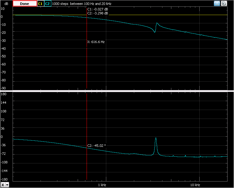
Ceramic Earphone Frequency Response
At first I thought the new earphone might not work well with a 1N34 crystal radio or the One Tube radio described in this article. However after constructing both and trying each headset in a blind test, I couldn't tell that there was a difference in sound volume.
So I decided to compare the sound pressure level from each earphone with a microphone, sweep generator, and spectrum analyzer set as flat as possible between 10 Hz and 10 kHz. As seen in the two images below, the new Amplified Parts earphone is more efficient at converting the sweep generator signal into sound. So I figured I was onto something.
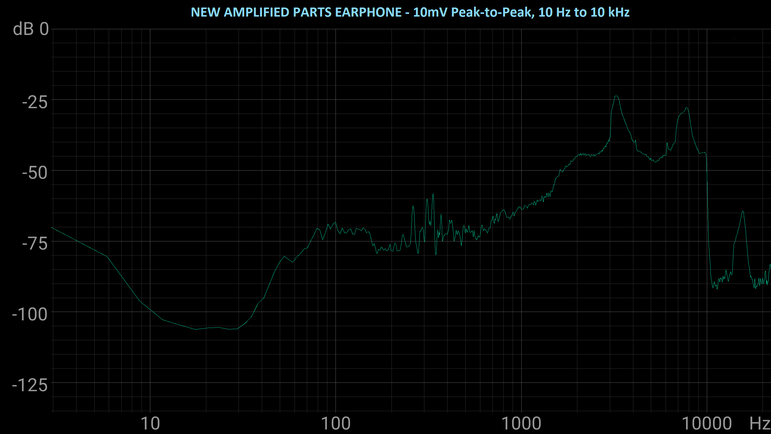
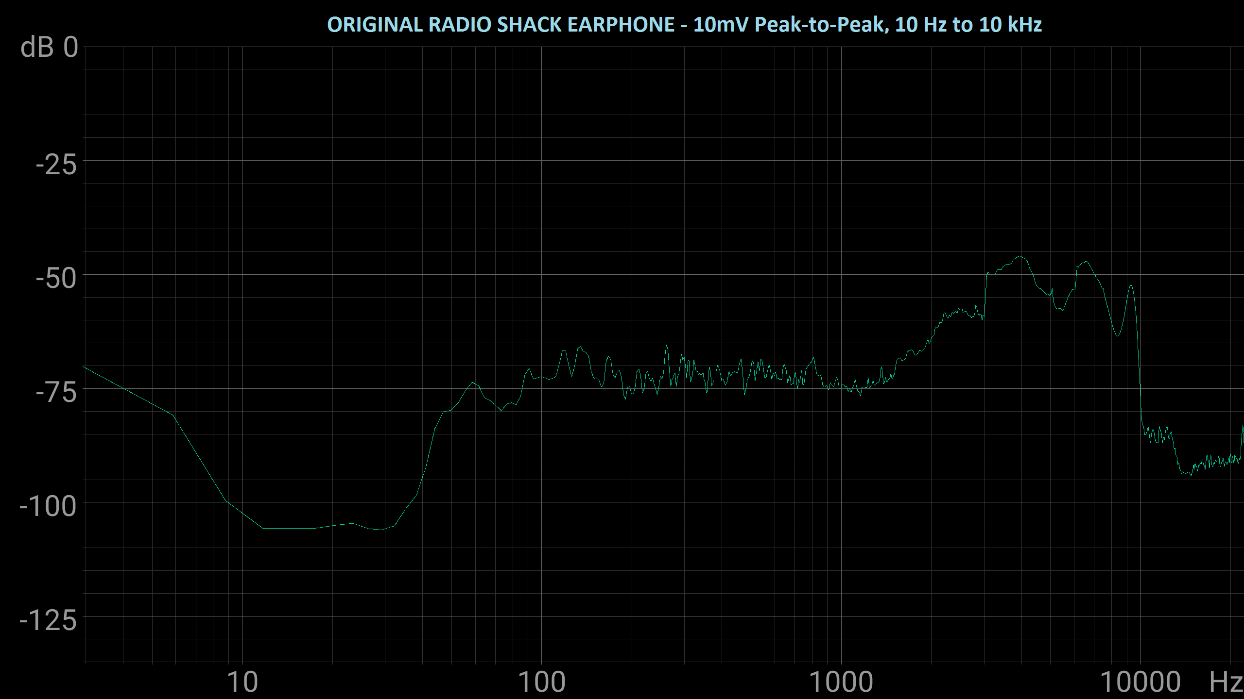
In the next test, I compared sound levels in a radio test circuit with 100K Ohms output impedance to see if there was a significant difference between the original Radio Shack earphone and the new Amplified Parts earphone.
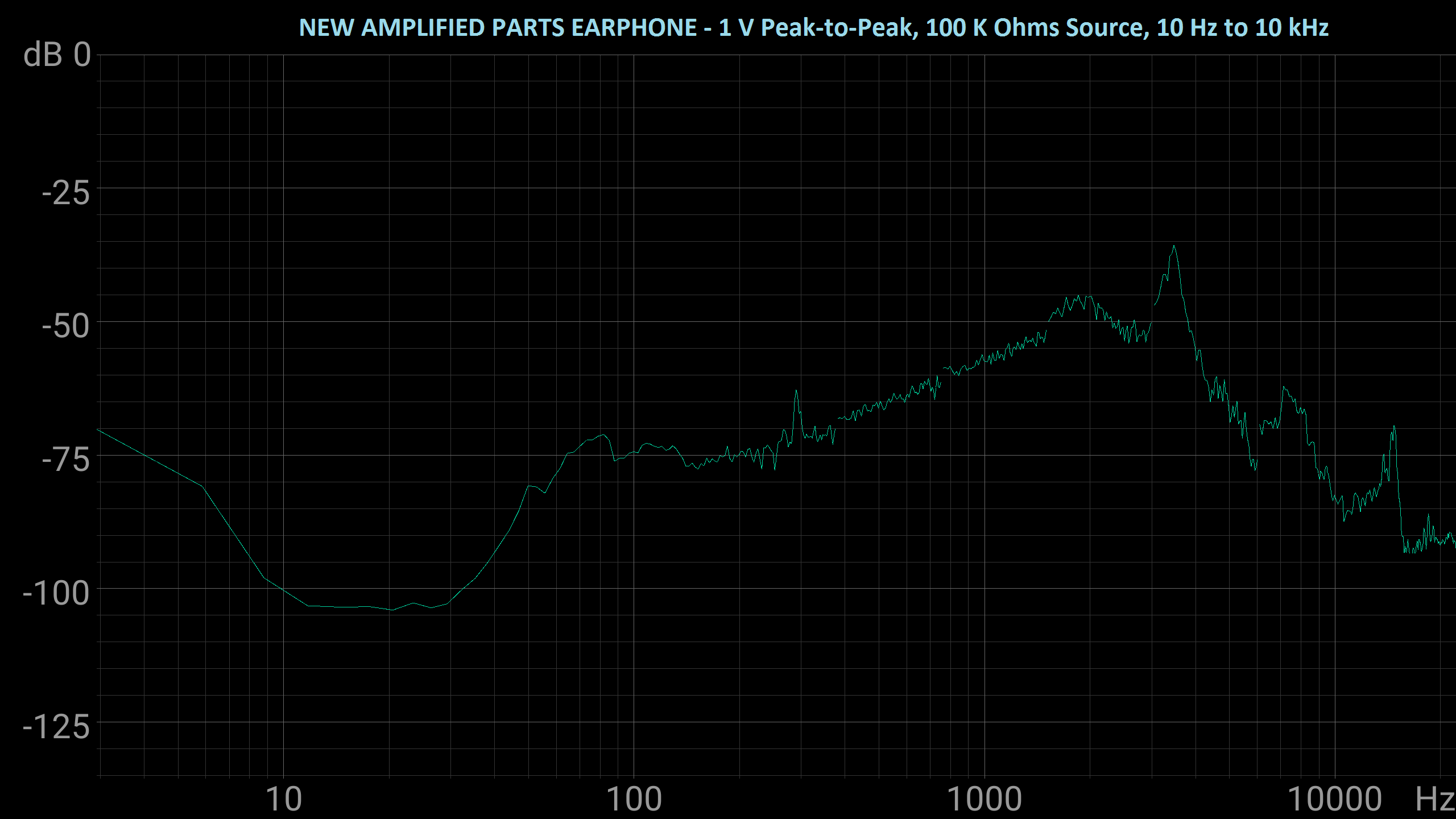
The Amplified Parts earphone loaded down my radio test circuit far more than the original Radio Shack earphone did, but appears to have almost made up for the impedance losses with conversion efficiency, which I think is why I'm not able to subjectively tell the difference between the two when doing a blind listening test.
ONE THING TO KEEP IN MIND, THOUGH:
I've bought several of these and had no issues up until just recently when one failed on me after a few days of radio listening. The two that are still working I've been using for over a year now. So I think there are some occasional quality issues with these that warrant getting more than one when building a project that uses them. I recently placed an order for three just to have extras on hand. You might want to do the same.
Review the Schematic to Become Familiar With the Radio Design
The original Radio Shack design used a variable inductance tuning coil and a fixed capacitor to form the LC parallel resonant tuning circuit. However that variable tuning coil is no longer available from a specialty electronic component retailer. However I was able to find a Miller-style P-C70-A antenna coil (sold by Amplified Parts) with sufficient inductance to permit a variable capacitor to set the LC resonant frequency in the AM broadcast band. The P-C70-A antenna coil has a similar appearance to the original Radio Shack part so I thought it would be fun to redesign the radio using available parts.
Tuning Section
L1 (primary) of the antenna coil is used to lightly couple the long wire antenna to the LC tuning circuit composed of L2 (secondary) and the parallel combination of variable capacitor sections C1, C2, and C3 (see the Varicap datasheet for more information). The ferrite alignment slug is adjusted so that the inductance of L2 is approximately 300uH. The trimmer capacitors of C1-C3 are adjusted to their minimum value so that the combination of C1-C3 provides a variable capacitance between 25pf and 300pF. Using the standard formula for parallel LC resonant frequency and plugging in the values for L and C results in the following tuning range:
Fc = 1 / [ 2 * pi * sqrt ( L * C ) ]
where L = .0003 Henrys and C varies between .000000000025 Farads and .0000000003 Farads.
Fc1 = 1 / [ 2 * pi * sqrt ( .0003 * .0000000003 ) ] = 530 kHz
Fc2 = 1 / [ 2 * pi * sqrt ( .0003 * .000000000025 ) ] = 1837 kHz
Since the medium wave broadcast band in ITU Region 2 (Americas) is 540 kHz and 1710 kHz with 10Khz spacing, my choice of inductor and capacitor worked out well for the tuner section (see block diagram above).
Detector Section
A popular AF detector in the 1920's was the grid leak detector composed of the 1T4 vacuum tube and the parallel combination of R1/C4. The Grid (Pin 6) and Cathode (Pin 1) of 1T4 form a diode that is forward biased by the B battery connected to L2. The large size of R1 (10 Meg Ohm) ensures that the Grid voltage with respect to the Cathode is held at approximately 0V with no signal. This causes the tube Cathode and Plate (Pin 2) to act almost like a closed switch resulting in a fixed voltage across resistor R1 of around 10V. When a station is tuned in, the alternating carrier wave received is directly coupled to the tube Grid (Pin 6) through capacitor C1. On the positive half cycles of the carrier wave the tube Grid is forced positive, but since the tube is already saturated almost no change in current occurs at the Plate output resulting in almost no voltage change across resistor R2. However, on the negative half cycles of the carrier wave, the tube Grid is forced negative which reduces the current across the Cathode/Plate resulting in a voltage change across resistor R2. The top half of the carrier is removed leaving the bottom half of the carrier intact with a copy of the audio signal modulated on it. The internal capacitance of the earphone (2500 pF) filters out the RF carrier wave leaving only the original audio signal. With the earphone connected, the audio signal voltage is converted into sound waves in the earphone that can be heard by the radio listener.
AF Amplifier Section
A basic operating characteristic of a vacuum tube is that small changes in Grid voltage result in large changes in Cathode/Plate current. When the Plate is connected to a load resistor like R2, large changes in Plate current cause large changes in load resistor voltage. Thus a small change in input voltage on the Grid results in a large change in output voltage on the Plate, which in electronics is called Amplification. The 1T4 vacuum tube works as an amplifying diode detector with a gain of around 100. This helps the radio perform better than a simple crystal radio.
Advantages of this radio design:
1. Relatively simple with few parts but better performance than the even simpler crystal radio.
2. Receives all local stations with a short 10' antenna and a ground connection.
Disadvantages of this radio design:
1. AC impedance of the grid leak detector loads the LC tuner which reduces selectivity of the radio.
2. Gain is insufficient for non-local stations. Regenerative radios achieve gains greater than 10,000 but add complexity to the circuit and station tuning process.
3. A grid-leak detector is easily overloaded by strong local stations resulting in noticeable distortion in the output. Making the antenna only as long as needed is important.
Review the Circuit Board Layout
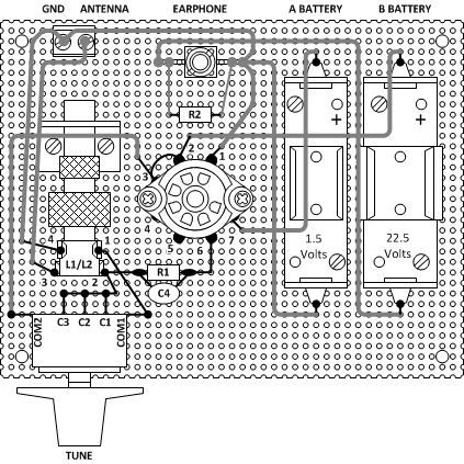
The Assembly Manual provides a step-by-step checklist for installing and soldering each component to the perfboard. I've used point-to-point wiring with 20 AWG solid hookup wire. Some of the connections can be made with just the component leads. Power, ground, and signal bus leads are best done with lengths of hookup wire. Parasitic capacitance isn't much of an issue for the frequencies this radio will operate at and I've already compensated for most of these in the design. When built, the radio is free of unwanted oscillation or noise.
When it comes to wiring, try to be as neat as I've indicated in the assembly manual. You don't have to be the world's best soldering artist but there's no good reason to do the work half-way. Go all out and make your radio look as good as you can.
Follow the Steps in the Assembly Manual to Complete the Radio
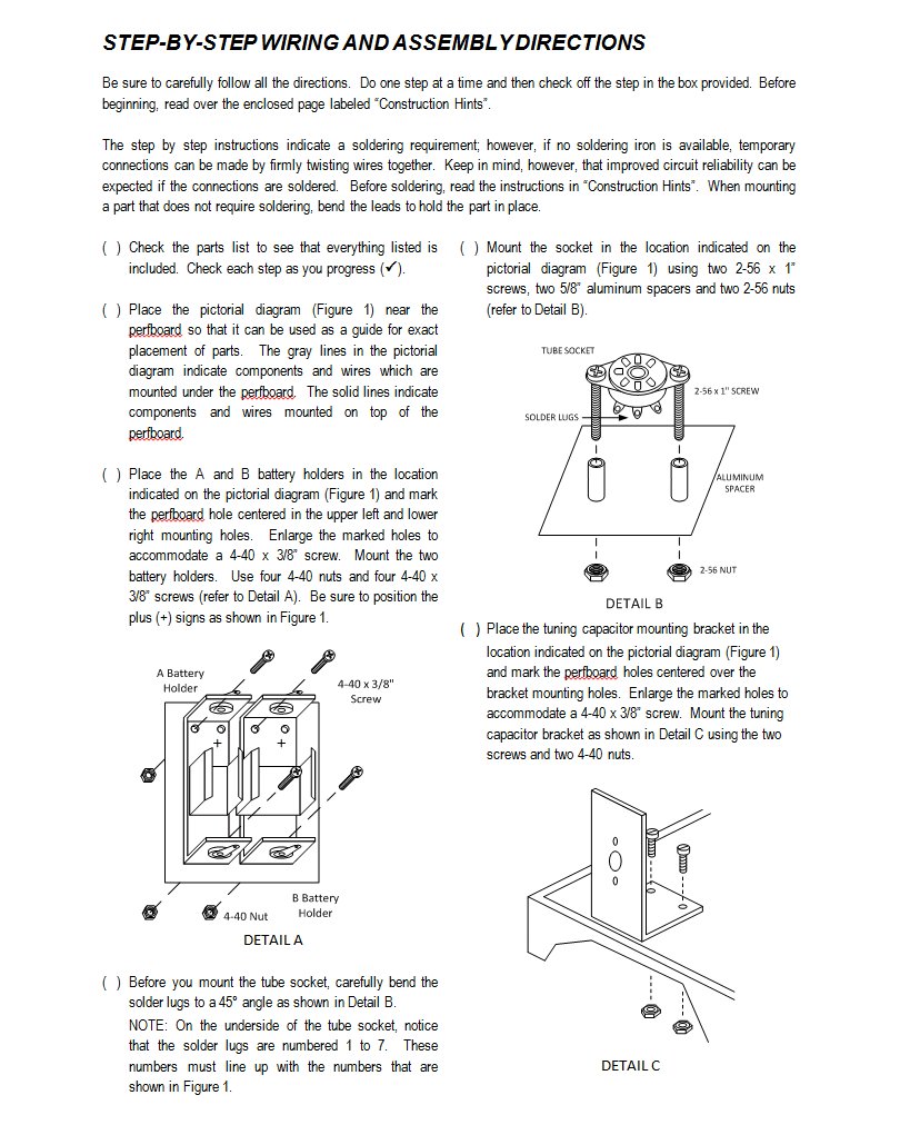
To make the assembled radio look more like the original Radio Shack PBOX kit, I purchased some flat red and satin clear spray paint. I've applied two coats of red and two light coats of clear which I think gives the perfboard a natural texture. Almost like it was made that way.
Use any color you wish but I recommend not skipping the clear coat if you paint the perfboard with flat colors. Flat paint tends to show marks and texture changes at the slightest touch. The natural vector board finish also looks nice so you don't have to use paint of you don't want to.
The perfboard specified in the parts list is too large to fit onto the Hammond case so some trimming is required as indicated in the images below. Follow the steps below to prepare the perfboard before installing components:
1. Using a sharp edge, carefully score the perfboard along the TOP ROW and BOTTOM ROW row of holes all the way to the end of the board. Run the sharp edge over the score line several times until it penetrates 1/4 to 1/2 way through the perfboard.
2. Using a sharp edge, carefully score the perfboard along the RIGHT COLUMN and LEFT COLUMN of holes all the way to the end of the board. Run the sharp edge over the score line several times until it penetrates 1/4 to 1/2 way through the perfboard.

Score edges of perfboard along dashed lines
3. Using a small pair of pliers, carefully bend the TOP ROW section back away from the score line. Work with one end of the TOP ROW, moving to the center, and then the other end. The TOP ROW section will eventually break away from the perfboard.
4. Using a small pair of pliers, carefully bend the BOTTOM ROW section back away from the score line. Work with one end of the BOTTOM ROW, moving to the center, and then the other end. The BOTTOM ROW section will eventually break away from the perfboard.
5. Using a small pair of pliers, carefully bend the RIGHT COLUMN section back away from the score line. Work with one end of the RIGHT COLUMN, moving to the center, and then the other end. The RIGHT COLUMN section will eventually break away from the perfboard.
6. Using a small pair of pliers, carefully bend the LEFT COLUMN section back away from the score line. Work with one end of the LEFT COLUMN, moving to the center, and then the other end. The COLUMN section will eventually break away from the perfboard.
Carefully break apart perfboard edges along score lines
7. Using an Exacto knife, match the trimmed perfboard with the Hammond case and enlarge holes at the corner to match with the corner mounting holes in the case. Work slowly and carefully with minimal pressure to avoid breaking the corner piece.
8. Place the potentiometer mounting brackets onto the perfboard and enlarge holes in the perfboard to match the holes in the brackets. Work slowly and carefully with minimal pressure to avoid cracking the perfboard.
Cut holes for case and bracket screws
9. Spray paint the perfboard with the color of your choice or leave it natural. It's your choice.

Paint with desired color
I typically use flat red followed up with 2 to 3 coats of gloss clear, but feel free to use any color that you like best.
When the perfboard is finished, follow the step-by-step instructions in the assembly manual <<< HERE >>>.
Installation of the Battery Holders
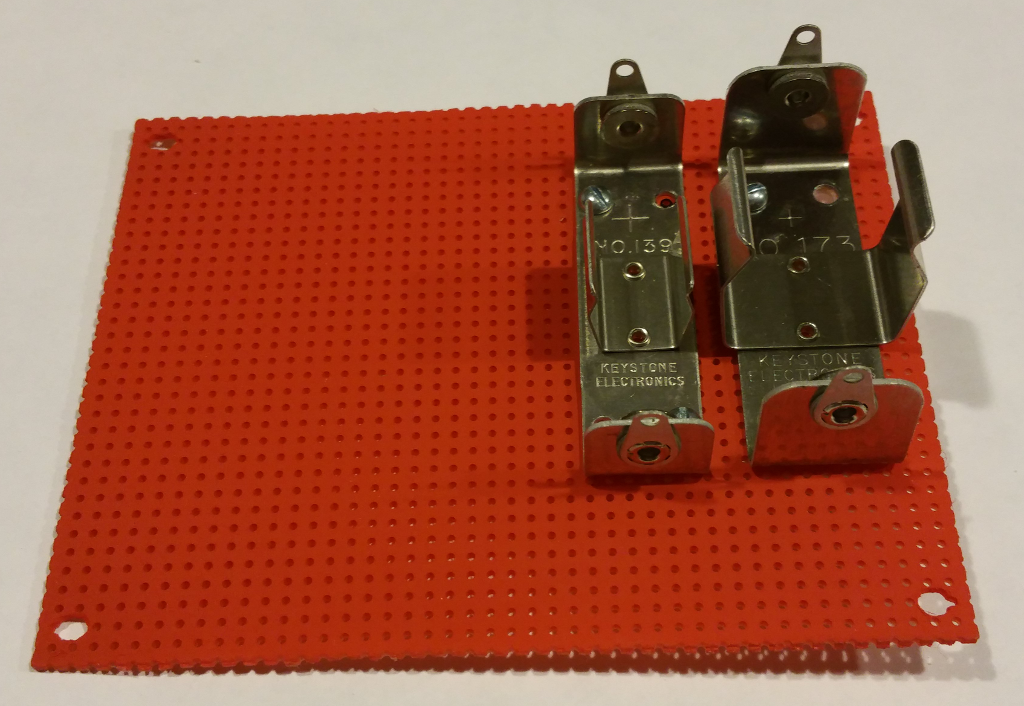
The above is what your radio should look like after the battery holders have been mounted. The battery holders have four screw holes in them, but you only need to use two screws to mount the holders to the perfboard: One in the upper left and the other in the lower right. I just placed the holders in position and marked the perfboard holes with a Sharpie pen. Next I used an Exacto knife to enlarge the holes. Use caution, work slowly, and watch the sharps!
Tube Socket Prepared and Mounted
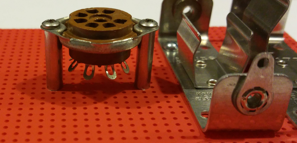
Before you mount the tube socket, very carefully bend the lugs out a little so that it is easier to attach wires to them and solder the connections. Don't do like I did my first time and break one off (man that was soul crushing). Just a little bend about 45 degrees is all that's needed.
Variable Capacitor Bracket Installed
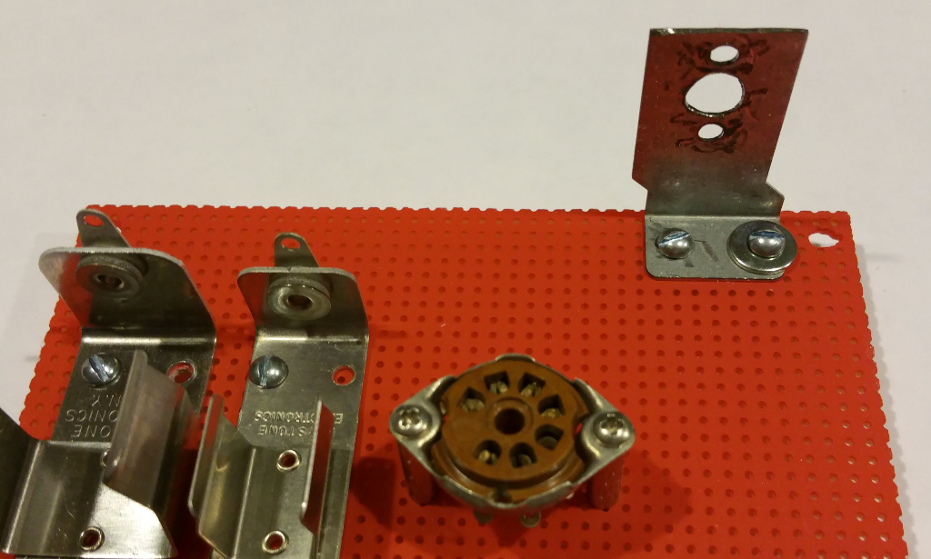
The above photo shows the variable capacitor bracket installed. Mine has the funny offset shape at the bottom because it's an old PC card slot blank. Yours will likely be different from mine depending on the materials you use. Just make sure it's tall enough so that the variable capacitor body will miss the perfboard mounting screws. And that the bracket is mounted close enough to the edge that the tuning knob can be tightened on the variable capacitor shaft without binding against the case. I've included a 1:1 scale drawing below to help you make brackets similar to mine.
Variable Capacitor Mounted on the Bracket
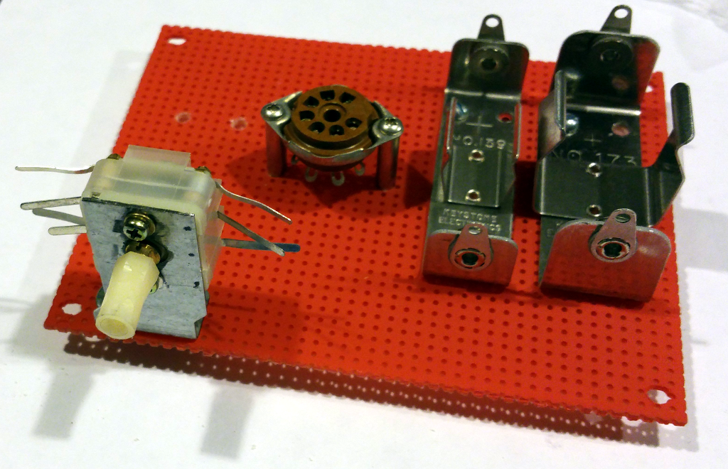
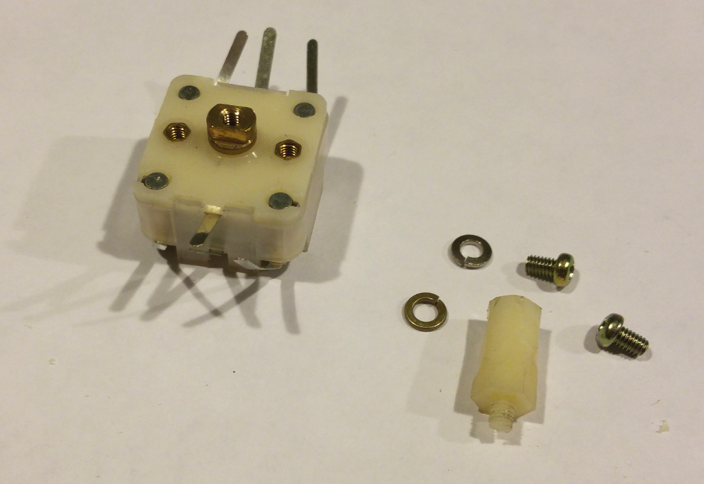
It's very important to use the proper screw length for the variable capacitor mounting holes. Screws that are too long will damage the variable capacitor. Always carefully test fit the screws to make sure they do not intrude into the case. Add some washers if you feel the screws may be too long based on the thickness of the material you use for the bracket.
I used an old nylon hex standoff from my junkbox for the variable capacitor shaft extension. The standoff was too thick to fit into the knob shaft so I whittled it down to size with an X-Acto knife, using extreme caution not to whittle down my thumb in the process.
Antenna Coil Bracket Mounted
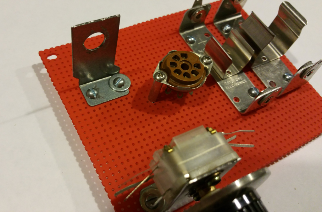
I test-fit the antenna coil in the bracket mounting hole before attaching the bracket to the perfboard. On mine I needed to expand the hole just a tiny bit and clean up the flash with my Dremel tool to get a nice tight fit. Don't push the antenna coil all the way in until the bracket is mounted or you might have trouble reaching the mounting screws. It's not easy getting the coil off the bracket once it's on.
Antenna Coil Mounted on the Bracket
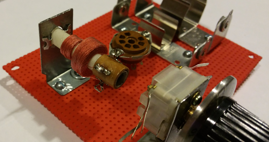
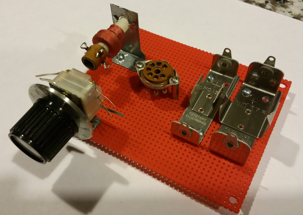
Now it's starting to look like the radio I remember. Be sure that the red dot on the antenna coil is facing directly toward the tube socket.
Soldering in the Grid Leak Detector Components
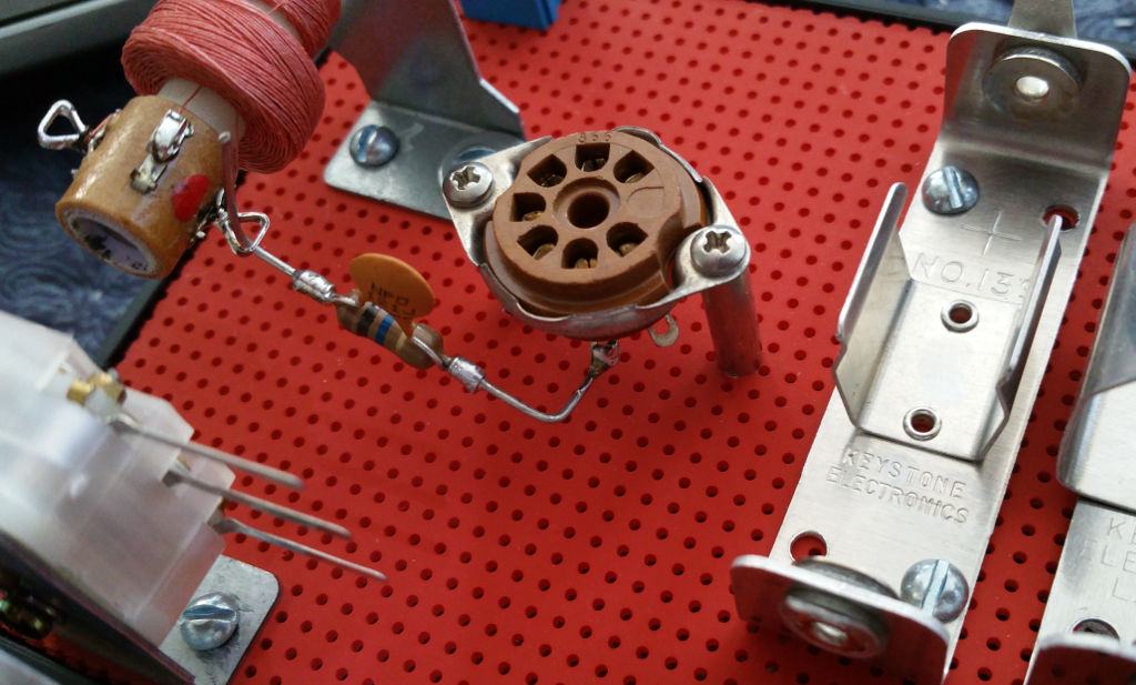
Just twist the capacitor leads around the resistor and solder. Then solder one end to tube socket pin 6. This is one of the hardest soldering tasks in this project. Once you have this and the rest of the tube socket pins soldered it's pretty easy to do the rest of the project.
A word from the soldering iron police: When you've finished using the soldering iron after turning it on, always remember to turn it back off again. If it's already off... then just walk away!
Solder Variable Capacitor Sections C1 Through C3 Together
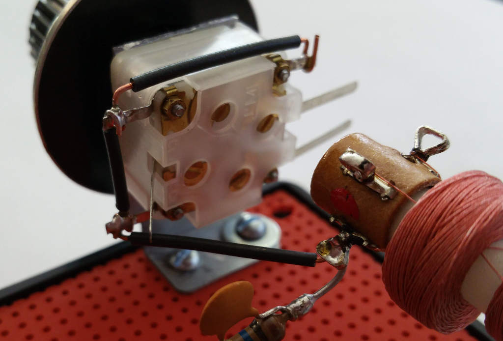
I've included a detail photo of this step as it might be a little more clear what's required and why. The variable capacitor for this project is actually 4 variable capacitor sections in one package. Two of the sections (C1 and C2) vary between 5pF and 135pF each. The remaining two sections (C3 and C4) vary between 5pF and 25pF. By combining these sections individually, in series, or in parallel you can make a variable capacitor with 10 different ranges (several of which are illustrated in the variable capacitor document included in an earlier step). These ranges can be fine tuned with 4 trimmer capacitors included on the back. This is a very versatile component, but it requires a little bit of wiring to get all the sections connected together the right way.
In this radio design we need to connect sections C1, C2, and C3 in parallel. If you observe the photo above, you can see that I have soldered a wire from the pin at the bottom left (C1) to the pin at the top left (C2). And I've soldered another wire from the pin at the top left (C2) to the pin at the top right (C3). The capacitor sections are all tied together internally at the three COM pins in the middle of the variable capacitor body. So by soldering these pins together, I have effectively placed capacitor sections C1, C2, and C3 in parallel. Since the values of capacitors in parallel add together, I've built a single variable capacitor with a range of 15pF to 295pF plus the value of the trimmer capacitors on the back which vary between 1pF and 10pF. In a previous step, I indicate how to set the trimmer capacitors to their minimum value, which makes the final capacitance range between 18pF and 298pF. The actual range will vary slightly due to manufacturing tolerances, but so will stray capacitance in the circuit you build. When doing the design calculations for tuning range, always allow for some room to adjust one way or the other.
The Finished Radio
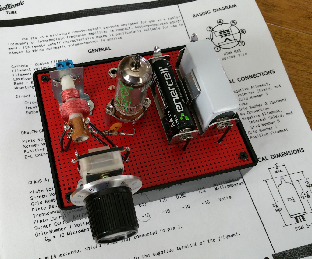
The assembly instruction document will walk you through each wiring step until your radio is completed and ready to power up. All you need to do when finished is double check your work to be certain everything is connected in the right place and well soldered.
After that, connect the antenna and ground connection, plug in the earphone, install the batteries, and tune in the stations.
I really like the look of the finished radio and am happy with it's performance. It's nowhere near as good as a modern superheterodyne, and not quite as good as a regenerative radio, but that's not the point. The point was to build a working radio of the type common in the early 1920's and get a sense for what it was like to use and listen to one; to walk in the footsteps of the people that invented radio. And, enjoy a useful device that looks vintage but is made by hand with off-the-shelf parts. The same way many radio amateurs did 100 years ago.
I hope you will enjoy this project as much as I have.
Some Comments About the AM Broadcast Band

Finding stations nearest you
If you are wondering what AM radio stations are nearest you, what frequencies they are broadcasting on, what content is broadcast, and what the operating daytime and nighttime power levels are then you might find the following FCC resource of interest:
https://www.fcc.gov/media/radio/am-query
By entering your city and state in the form, you can select a simple or detailed listing of the stations in your area. For example, in my city of Austin, TX there are three stations nearby that broadcast 24 hours a day on 590 kHz, 1300 kHz, and 1490 kHz. I was able to receive these three stations during the day, but two of them were stronger. After reviewing the list the reason was obvious: Two stations (KJBJ and KVET) are licensed for 5KW. The third station (KTAE) is licensed for only 1KW.
You can look up the station service area map to see how strong the radio signal is in your area (see image above). And you can find out more information about the station such as the current owner, number and location of antennas, how long the station has been licensed, how station ownership has changed over time, and probably a lot more than you want to know about a radio station.
I use the FCC data to determine what to expect from the radio's I build and whether or not my tuning is on target.
AM Broadcasts during the Day
During the day, ultraviolet radiation from the sun causes heavy ionization of three layers within the upper atmosphere (the ionosphere). The lowest layer, called the D layer, easily absorbs the energy of AM radio waves and confines AM broadcasts closely to the surface of the earth. These AM "ground waves" are attenuated as they pass over the surface of the earth depending on soil conductivity (sea is best, cornfield is good, city is worst), and are gradually refracted into the earth where they are eventually absorbed. The result is that useful daytime AM radio service is limited to a radius of no more than about 100 miles. If you were wondering why your homemade AM radio can't pick up anything but nearby stations, it's not your radio. It's the way AM works. During the day.
AM Broadcasts at Night
At night when ultraviolet radiation from the sun is no longer present, the D and E layers of the ionosphere almost disappear leaving only the F layer, which due to height and composition make it an excellent reflector of radio waves below 10 MHz. At night, AM radio waves can travel high into the atmosphere and be reflected back to earth hundreds of miles away. These AM "sky waves" could cause massive interference if every station were to transmit at full daytime power. To prevent this, the FCC requires most stations to reduce transmit power at night. For example, in my area there are two stations licensed for 5KW during the day, but only 1KW at night. The exception to this rule are Clear Channel stations (not to be confused with the former Clear Channel Communications company now known as iHeartMedia Inc). Clear Channel stations were licensed under FCC intent to provide radio service to rural areas and create a cross-country communications system for use in the event of a national emergency. In the US, all Clear Channel stations are limited to a maximum power of 50KW. However, in Mexico many Clear Channel stations operate at 100KW and higher, which is why you have a good chance of receiving music and news from Mexico City at night.
Troubleshooting Your Radio
If you build the radio and don't hear anything, immediately remove the batteries and try the following checklist to find the problem:
1. Test the earphone. With a multimeter set to Ohms and the earphone loosely in your ear, measure the resistance across the earphone jack conductors. If you hear a slight clicking sound touching the multimeter leads to the earphone jack conductors, the headphone is most likely working.
2. Verify that the batteries were inserted correctly. The (+) end of each battery points at the top of the radio when the tuning knob is facing you. Insert the batteries in the direction indicated and test station reception again. If you don't hear a station, immediately remove the batteries.
3. Insert the batteries in the battery holder and use a multimeter set to DC Volts to check the voltage on each battery by measuring from the battery holder lugs. If you do not observe approximately 1.5V across the A Battery and approximately 22.5V across the B Battery, immediately remove the batteries and check for loose connections or solder at the battery holders. If there are no wiring errors, one or both batteries may be dead or damaged. Insert fresh replacement batteries and repeat Step 3.
4. With a multimeter set to Ohms and the A and B batteries removed, check the resistance across the A Battery holder terminals. If you observe a high resistance greater than 40 Ohms, double check the A Battery wiring with the assembly manual. Look for miswiring, cold solder joints, missing solder, broken wire, or other wiring related problem. If you observe 0 Ohms on the multimeter, remove the 1T4 tube from its socket and take the measurement again. If you still observe 0 Ohms on the multimeter, double-check all wiring for errors and look for any solder bridges, wire clippings, or unclipped wires under the tube socket. If the multimeter only measures 0 Ohms with the 1T4 tube inserted, the 1T4 tube may be bad. Insert a replacement 1T4 tube and repeat Step 4.
5. With a multimeter set to Ohms and the A and B batteries removed, check the resistance across the B Battery holder terminals. If you observe anything other than a very high reading (1 Meg Ohm or higher), double-check all wiring for errors and look for any solder bridges, wire clippings, or unclipped wires under the tube socket.
6. Verify the 1T4 tube is inserted fully in it's socket and then Insert the A and B Batteries into the battery holder. Wait 5 seconds and then with a multimeter set to DC Volts, measure the voltage across 270K resistor R2. Remove the A and B Batteries. The measured voltage should have been between 9V and 12V. If the measured voltage was not within this range, check the color codes on R1 and R2 to verify they are the correct value. Double-check all wiring and verify no bad solder joints, missing solder, loose connections, or broken wires are found.
7. Using a multimeter set to Ohms, check the resistance across tuning coil L1. The resistance of L1 should be approximately 42 Ohms. If the multimeter measures much less than 42 Ohms or 0 ohms, double-check all wiring at the antenna coil. Look for hard to see solder bridges, wiring errors, wire clipping, or unclipped wires touching. If all wiring is correct, unsolder one of the wires to L1 and measure the resistance of L1 again. If the measured resistance is still much less than 42 Ohms then the tuning coil is likely bad. Replace the tuning coil, insert batteries and the earphone, and try to receive a station. If the measured resistance of L1 is very high (> 100 Ohms), then the antenna coil is likely bad. Replace the tuning coil, insert batteries and the earphone, and try to receive a station.
8. Using a multimeter set to Ohms, check the resistance across tuning coil L2. The resistance of L2 should be approximately 10 Ohms. If the multimeter measures much less than 10 Ohms or 0 ohms, double-check all wiring at the antenna coil. Look for hard to see solder bridges, wiring errors, wire clipping, or unclipped wires touching. If all wiring is correct, unsolder the wire from the Variable Capacitor COM pin to Pin 1 of L2 and measure the resistance of L2 again. If the measured resistance is still much less than 10 Ohms then the tuning coil is likely bad. Replace the tuning coil, insert batteries and the earphone, and try to receive a station. If the measured resistance of L2 is very high (> 100 Ohms), then the antenna coil is likely bad. Replace the tuning coil, insert batteries and the earphone, and try to receive a station. If the measured resistance of L2 with Pin 1 unsoldered from the variable capacitor is approximately 10 Ohms, verify all wiring at the variable capacitor. If all wiring is normal, the variable capacitor may be shorted. Remove the variable capacitor and verify that the mounting screws are not too long. Check the resistance of each capacitor section between C1, C2, C3, C4, and COM. If any capacitor section measures 0 Ohms, replace the variable capacitor.
Build a Neon "Goofy-Lite"
Occasionally I encounter a circuit that is schematically simple but challenging in theory, yet has no practical purpose other than to look cool. Every electronics lab needs a black box with blinking lights hanging around in a corner somewhere. Just about every science fiction movie or television show ever made has blinking lights of one type or another. The Neon Goofy Lite project described in this article is easy to build but contains enough interesting parts, theory, and history to start conversations and invite questions from expert and novice alike. The version covered here has been running non-stop making that vintage orange neon glow for over two weeks on four AA batteries.
Between 1968 and 1970, Radio Shack offered 28 project kits designed to introduce customers to breadboard construction techniques and electronics theory. By 1971 there were 26 P-Box kits to choose from and many pages of electronic components, tools, and educational project labs. Unfortunately, after 1974 Radio Shack's preoccupation with Arthur Fiedler, stereo electronics, and CB radio gradually reduced the size of the electronic components and kits section of the catalog. In 1979 there were only six remaining P-Box kits offered and by 1980 they were dropped from the catalog entirely, replaced by printed circuit "kits" that were not as interesting and more than 3 times the cost of the most expensive P-Box project.
In honor of a great set of educational Radio Shack electronics project kits available during the 60's and 70's, I've redesigned the original Science Fair brand Neon Goofy Lite (Catalog #28-130) using modern components still available from electronics component re-sellers in the US. All of the components in the updated kit can be found at Mouser or Digikey. There were many things Radio Shack did extremely well during its prime. For the nostalgic or the enthusiast who would like to build an updated version of this classic "blinking light" kit, I've included schematics, parts information, assembly documentation, and pictures of a completed and tested Neon Goofy Lite based on the original from 1970.
Obtain The Assembly Manual
The Neon Goofy Lite project described here is based on the Radio Shack pbox kit of the same name, but it has been updated with silicon transistors and passive components that can be obtained from electronics suppliers like Mouser and Digikey. I've built the updated Neon Goofy Lite kit described here and believe it works just as well as the original kit did back in 1970. To make it easy to replicate my work, I've provided illustrations and step-by-step assembly documentation based on the original assembly manual from Radio Shack.
To build the kit, you will need the revised assembly manual available >>> HERE <<< .
I've kept the original branding and publishing style of the Science Fair Neon Goofy Lite in order to preserve the original look and feel of the documentation set for the builder. But every page has been updated to reflect the changes I've made in order to incorporate modern and available parts.
Obtain Components On The Parts List
Review the parts list and obtain the components indicated. All components are available from Mouser or Digikey, or can be obtained from other suppliers that may be more convenient to your geography. Total cost is just less than $27. To put that cost in perspective, the Goofy Lite kit was introduced in 1970 at a retail price of $6. The economic value of $6 in 1970 is equivalent to $44 today. The project described in this article can be built for about half the cost of the project kit offered by Radio Shack in 1970. But keep in mind that Radio Shack needed to make a profit from the sale of their kit which explains where the other half of the cost went.
Below are a few notes regarding the parts used for the Goofy Lite project:
1. The resistors for the project can be purchased from Mouser or Radio Shack (assuming they are still in business in your area). But I highly recommend the excellent Joe Knows Electronics resistor kit. It includes the resistors you need for this project and over 860 different values that can be used for other projects, all labeled in individual plastic packages for just $17. For this project you can use 1/4W or 1/2W resistors. It's your choice. Check out www.joeknowselectronics.com. You will not be sorry.
2. The case for the Goofy Lite project I built is a Hammond 1591GSBK ABS Project Box from Mouser. I used a piece of vector breadboard cut to fit on the top and spray painted with high temperature automotive flat red. I like the look of red on black, and the red color of the breadboard matched the red color of the original pbox kit. It's completely up to you how you want to house and color the kit you build.
3. The original pbox kits used tin-plated spring clips for attaching the battery holder to the perf-board enclosure. These clips were a pain to solder to when new and they tarnished like crazy after they were installed resulting in intermittent connections. Fortunately for everyone they are no longer available. I am continuing to experiment with different connector types that are small and inexpensive. For this project I found some small screw connectors from Mouser (part number 534-8730). They aren't perfect but they are very small and make consistently good connections. Feel free to use the battery connector of your choice and let me know if you find something that works really well for you.
4. The original pbox kit used an audio coupling transformer for T1. This coupling transformer is no longer available from the original manufacturer or any alternative source I could find. Fortunately it was quite easy to find a suitable replacement transformer of equivalent turns ratio from Hammond Power Solutions (Mouser Part 546-161C10). This transformer is roughly twice the size of the original Radio Shack transformer but performs much better in my opinion. The only disadvantage is that the Hammond transformer core doesn't whine like the old audio transformer used to. It's very effective but completely silent.
5. Pay particular attention to the voltage rating of the capacitors. This project generates up to 130V DC on the T1 secondary in order to ionize the neon gas in the lamps. Don't use capacitors less than 200V DC for C1 through C5.
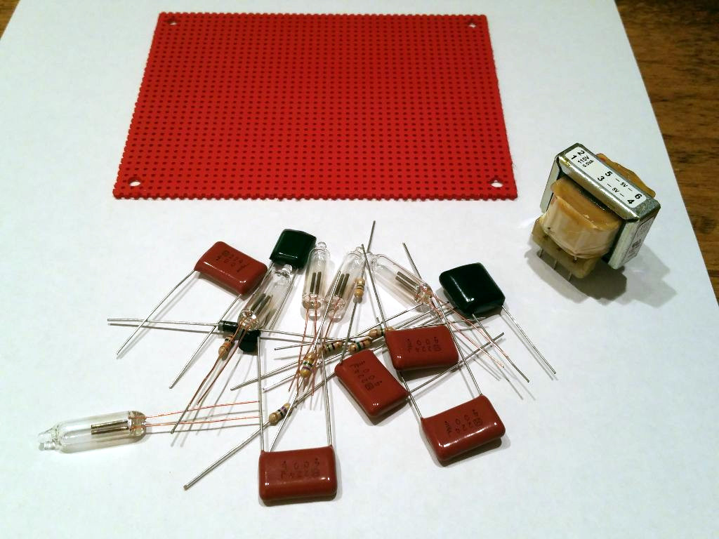
CAUTION: Although the current generated by T1 is extremely low and considered harmless, don't go out of your way to touch components on the high voltage side of the circuit when it is running. Don't take this circuit with you to the tub to see if it will float while you are taking a bath. Don't try to shock your friends with it. Treat all electronic circuits with the respect they deserve.
Please Note: I have no business relationship with any of the above vendors. Nothing of financial value was exchanged for my recommendation. None of the above vendors provided compensation of any kind during the creation of this project. I will not be compensated in any way if you choose to build this project or purchase components from any vendor I recommend. I simply had a good experience with the vendors I recommend and believe you will too.
Review the Schematic to Become Familiar With the Goofy Lite Design
You have a decision to make, which is actually pretty cool since most projects can only be constructed one way and can only do one thing. But the Neon Goofy Lite project is more flexible than that. It is possible to configure the project to flash the 5 neon lamps in a pseudo-random pattern or a sequential pattern. I built both circuit types and liked the pseudo-random pattern the best (see the video on the summary page) but your preference may be different from mine. The assembly manual covers both types in detail so it's entirely up to you which circuit you build.
The Goofy Lite circuit looks simple but contains enough theory to keep a second year engineering student busy. The core of the circuit is a negative resistance device: The NE2 neon lamp (also known as the A1A lamp). There aren't many devices in electronics that exhibit negative resistance; a few microwave diodes, SCRs, the uni-junction transistor, and gas discharge tubes like the neon lamp. The great thing about a negative resistance device is that it can be used to build a simple oscillator with only a couple of passive components. No amplifiers or feedback networks required.
Negative Resistance
To get an idea of what is meant by "negative resistance", review the two V/I charts below. The first represents a V/I graph of a diode and a resistor, both positive resistance devices you are probably already familiar with. The second represents the V/I graph of a neon lamp, a negative resistance device. Notice in the positive resistance graph that the slope of the V/I curve is always positive (up and to the right). Increasing current through the device always results in an increasing voltage drop across the device. However, notice that the neon lamp has a portion of its V/I curve with a negative slope at the lamp breakdown voltage (90 volts). In the negative slope region, increasing current through the lamp results in a decreasing voltage across the lamp. This characteristic is what makes the blinking neon lamp in the Goofy Lite project possible.
In the 50's and 60's, neon lamps were used to build all sorts of interesting circuits including oscillators, timers, binary counters, binary dividers, lamp dimmers, and light detectors. The only disadvantage with neon lamps today is their high voltage requirement (60V to 150V). But in the past, these voltages were common for electron tube (valve) circuits making it very easy to use a neon lamp. Review the two neon lamp circuit diagrams below. One is a Relaxation Oscillator circuit and the other is a Multivibrator circuit. The Relaxation Oscillator is used in the Random version of the Goofy Lite project. The Multivibrator is used in the Sequential version of the Goofy Lite project. Below is a description of how each circuit works:
Neon Lamp Relaxation Oscillator
In order to control the flash rate of the neon lamp, we need a time delay. A simple time delay circuit can be constructed with a resistor and a capacitor in series, often referred to as an RC circuit. When energized, the capacitor gradually charges to near the power supply voltage. How quickly the capacitor charges is determined by the value of the resistor and the value of the capacitor according to the following formula:
Trc = R * C
Refer to the Relaxation Oscillator Schematic below. When power as applied to the series circuit C1/R1, capacitor C1 will begin to charge. When C1 voltage reaches the neon lamp firing voltage (90V), the neon lamp will light and C1 will discharge into the neon lamp. Resistor R1 will essentially be isolated from the circuit due to the relatively low resistance of the neon lamp. When C1 voltage falls below the neon lamp holding voltage (50V), the neon lamp will extinguish and C1 will begin charging again through R1. This cycle will repeat for as long as power is applied to the circuit.
Review the chart underneath the Relaxation Oscillator Schematic. The chart contains the capacitor voltage over time. Notice that the capacitor does not charge in a straight line but in an exponential curve function. The equation for this curve is:
Vcapacitor = Vpower * [ 1 - e^(-t/RC)]
You might recognize this equation if you've had a class in statistics, physics, or calculus. This equation is very easy to use with a modern calculator so don't let it intimidate you. Solving the equation for the resistor and capacitor values RC will render it a little more useful when designing circuits like the Goofy Lite:
RC = -t / ln (( Vf - Vh ) / Vf )
In the above equation, ln is the natural log function on a calculator, Vf is the neon lamp firing voltage, Vh is the neon lamp holding voltage, t is the desired lamp flash rate, and RC is the product of the capacitor and resistor needed to produce a flash rate of time t.
For example, I wanted a flash rate around 1 second for each lamp so I used the following:
Lamp Firing Voltage = 90 VDC
Lamp Hold Voltage = 50 VDC
RC = -1 / ln (( 90 - 50 ) / 90 ) = 1.23
I wanted to keep the .22uF capacitor values used by the original P-Box kit, so all I needed to do was divide the RC value by .00000022 Farads in order to obtain the value for the resistor:
R = 1.23 / .00000022 = 5.5 Megohms
The nearest standard resistor value I had in inventory was 4.7 Megohms so I used that for the resistor values in the random circuit.
The reason this circuit is referred to as "Random" is that the flash rate for each neon lamp will vary depending on the tolerance of the capacitors, resistors, and lamps. Many capacitors have a tolerance of 10% and 20%. The resistors I used were 5% tolerance. The neon lamps seem to have firing and hold voltages that varies as much as 20%. All of these tolerances combined will vary the actual neon lamp flash rate between .8 seconds and 1.2 seconds. Sometimes more. This results in what appears to the eye to be a random flash pattern among the 5 neon lamps. If you focus on one lamp you will see that the flash rate is actually fixed for that lamp. The other lamps are firing at different rates which creates the illusion of a random flash pattern.
Neon Lamp Sequential Multivibrator
All of the principles described above apply to the sequential circuit. The only difference is where the capacitors are attached. The sequential version of the Goofy Lite is composed of several Multivibrator circuits distributed among the 5 neon lamps. Review the sequential circuit diagram below and the chart attached to it.
When power is applied, one of the neon lamps will immediately fire first due to manufacturing tolerances. In this description, lets assume that neon lamp NE2-1 fires first. When NE2-1 fires, it creates a conductive path for capacitor C1 to charge. When the voltage on C1 reaches the firing voltage of NE2-2, that lamp will fire which causes the voltage on C1 to extinguish neon lamp NE2-1. C1 will then charge through the conductive path provided by NE2-2 until it approaches the firing voltage of NE2-1. NE2-1 will then fire causing the voltage on C1 to extinguish neon lamp NE2-2. This cycle will repeat for as long as power is applied to the circuit.
By carefully distributing three copies of the Multivibrator circuit among the 5 neon lamps, the sequential circuit can be made to flash each neon lamp one after the other.
DC-DC Step-Up Converter
If all the above theory wasn't enough, we still need some way of producing 150V DC from a set of AA batteries. The original P-Box kit used an audio transformer with a 24:1 turns ratio to step up the 6 VDC battery voltage to around 150 VDC for the neon lamps. However that audio transformer is no longer available from any commercial source (I've tried them all). Occasionally someone on eBay will offer one for sale from an estate auction, but you can't buy these in volume from any commercial company. An acceptable solution to this problem turns out to be very simple. Any step-down power transformer can be used as a step-up power transformer when the primary and secondary windings are transposed. All I needed to do was find the smallest step-down power transformer commercially available that provided a turns ratio of around 24:1. It turns out that Hammond Power Solutions makes a small transformer with a 115V primary and dual 5V secondaries which is just perfect for the Goofy Lite project. The Hammond transformer is about twice the size of the original Radio Shack audio transformer but is still quite small and performs extremely well as a substitute.
The DC-DC Step-Up Converter is actually a classic Blocking oscillator which uses a tapped primary inductor for the energizing and feedback circuits. All I needed to do was connect the Hammond transformer secondary coils together so that they appeared to Q1 as a tapped inductor. R6 is a current limit for the base of Q1 while C7 ensures that the base of Q1 gets a "kick" when power is first applied to ensure that the DC-DC converter circuit starts oscillating. The second secondary winding of T1 provides the positive feedback signal to Q1 which keeps the DC-DC converter circuit oscillating. C6 isolates the feedback winding of T1 from the 6V battery so that only the feedback signal controls the operation of Q1.
When power is first applied, the base of Q1 will be tied briefly to V+ which immediately saturates Q1 and starts current flowing through the first secondary winding of T1. Feedback from the second secondary winding will begin to reverse bias Q1 resulting in less current through the first secondary winding. When Q1 becomes turned off, the combination of R6/C7 will begin turning Q1 back on again and the entire cycle will repeat as long as power is applied. The frequency of oscillation for the converter is around 135Hz.
The number of wire turns in the primary coil of T1 are 23 times higher than the number of turns in the secondary coils. This multiplies the voltage applied to the secondary coils attached to Q1 by 23 resulting in a voltage to the neon lamps of approximately:
Vsecondary * Turns_Ratio = Vprimary
6 VDC * 23 = 138 VDC
This is more than enough to run both the random and sequential versions of the project. Average current consumption is 18mA so a set of four AA batteries should run at least two weeks non-stop.
Hopefully this section has helped you understand how the Goofy Lite circuit was designed and how it operates.
Review the Circuit Board Layout
The Assembly Manual provides a step-by-step checklist for installing and soldering each component to the vector board. As you can see from the opposite side illustration of the vector board, I've used point-to-point wiring with 22 AWG solid hookup wire. Most of the connections can be made with just the component leads. But power, ground, and signal bus leads are best done with lengths of hookup wire. There are two versions of the Goofy Lite project. I've built the Random version and illustrated the opposite side of the circuit board. The sequential version will be very similar.
When it comes to wiring, try to be as neat as I've indicated in the assembly manual. You don't have to be the world's best soldering artist but there's no good reason to do the work half-way. Go all out and make your project look as good as you can.
Follow the Steps in the Assembly Manual to Complete the Goofy Lite Project
Before you begin:
The perfboard specified in the parts list is too large to fit onto the Hammond case so some trimming is required as indicated in the images below. Follow the steps below to prepare the perfboard before installing components:
1. Using a sharp edge, carefully score the perfboard along the TOP ROW and BOTTOM ROW row of holes all the way to the end of the board. Run the sharp edge over the score line several times until it penetrates 1/4 to 1/2 way through the perfboard.
2. Using a sharp edge, carefully score the perfboard along the RIGHT COLUMN and LEFT COLUMN of holes all the way to the end of the board. Run the sharp edge over the score line several times until it penetrates 1/4 to 1/2 way through the perfboard.
Score edges of perfboard along dashed lines
3. Using a small pair of pliers, carefully bend the TOP ROW section back away from the score line. Work with one end of the TOP ROW, moving to the center, and then the other end. The TOP ROW section will eventually break away from the perfboard.
4. Using a small pair of pliers, carefully bend the BOTTOM ROW section back away from the score line. Work with one end of the BOTTOM ROW, moving to the center, and then the other end. The BOTTOM ROW section will eventually break away from the perfboard.
5. Using a small pair of pliers, carefully bend the RIGHT COLUMN section back away from the score line. Work with one end of the RIGHT COLUMN, moving to the center, and then the other end. The RIGHT COLUMN section will eventually break away from the perfboard.
6. Using a small pair of pliers, carefully bend the LEFT COLUMN section back away from the score line. Work with one end of the LEFT COLUMN, moving to the center, and then the other end. The COLUMN section will eventually break away from the perfboard.
Carefully break apart perfboard edges along score lines
7. Using an Exacto knife, match the trimmed perfboard with the Hammond case and enlarge holes at the corner to match with the corner mounting holes in the case. Work slowly and carefully with minimal pressure to avoid breaking the corner piece.
8. Place the potentiometer mounting brackets onto the perfboard and enlarge holes in the perfboard to match the holes in the brackets. Work slowly and carefully with minimal pressure to avoid cracking the perfboard.
Cut holes for case and bracket screws
9. Spray paint the perfboard with the color of your choice or leave it natural. It's your choice.
Paint with desired color
I typically use flat red followed up with 2 to 3 coats of gloss clear, but feel free to use any color that you like best.
Assembly Photos - DC/DC Step-Up Converter
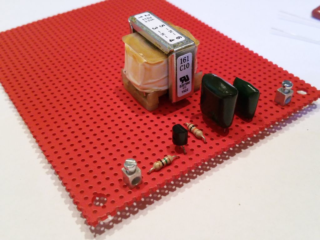
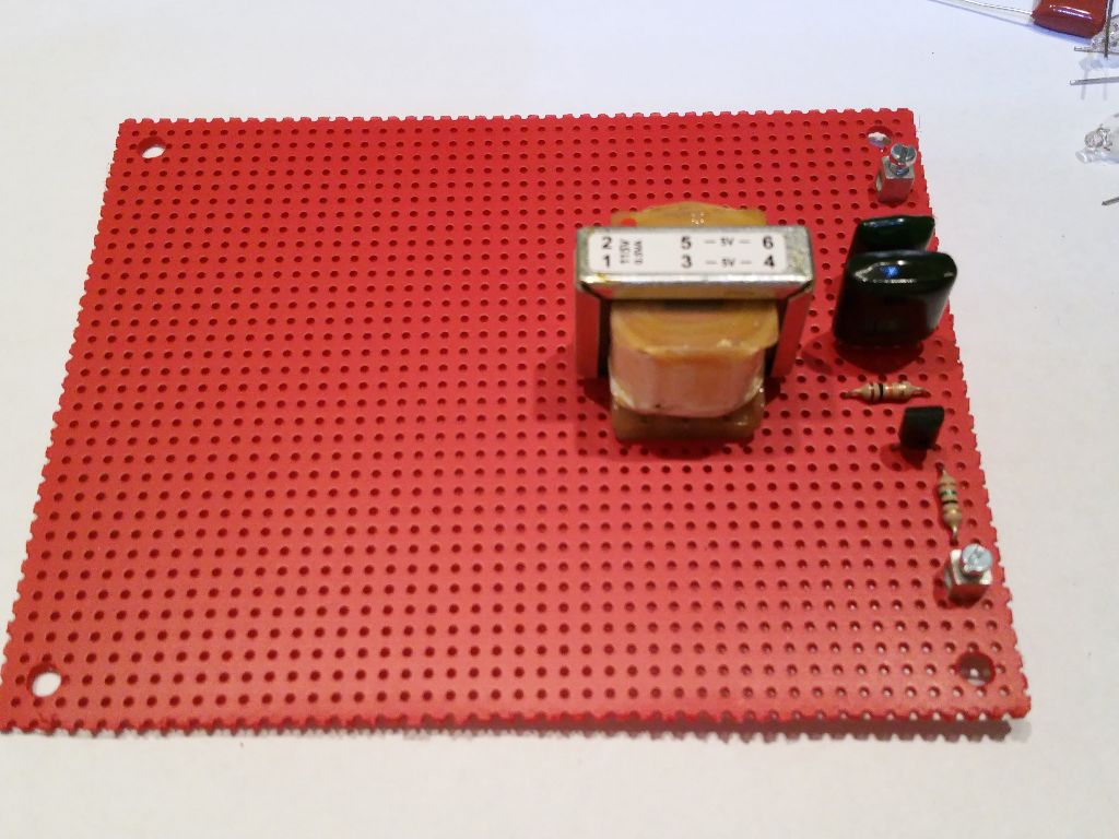
After Step 12 in the Assembly Document, the Goofy Lite project should look something like the photos above.
Assembly Photos - Neon Lamp Section
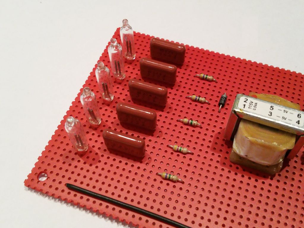
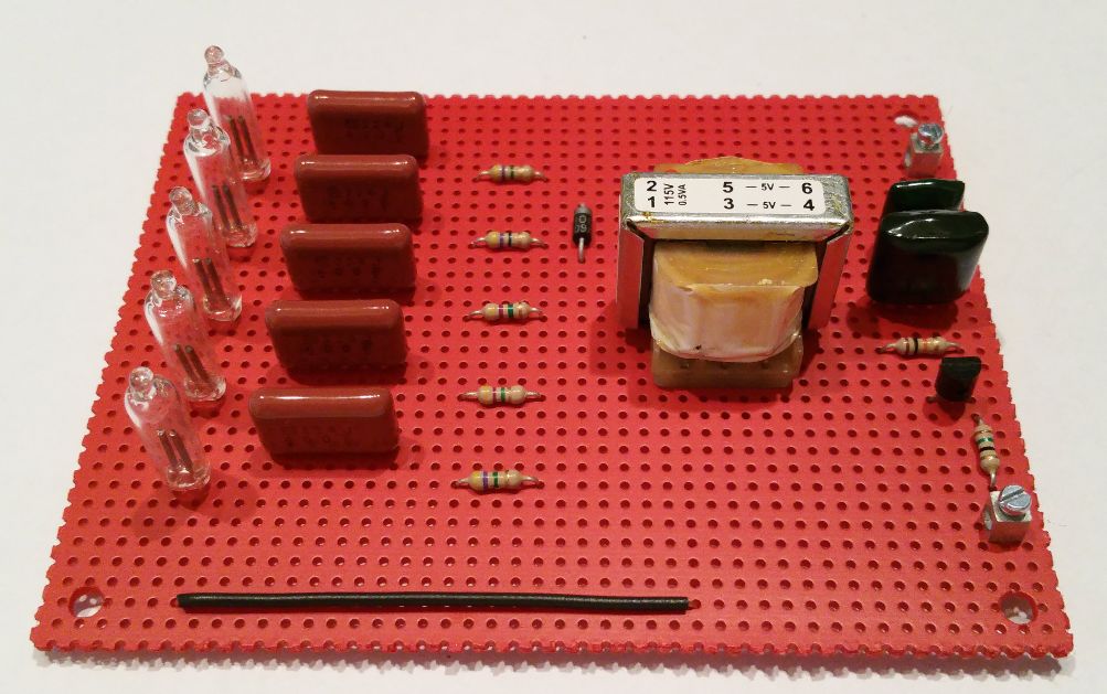
After Step 28 in the Assembly Document, the Goofy Lite project should look something like the photos above.
Note: Capacitors C1 through C7 will be in a different location depending on the version of the project that you build. What is shown is the Random layout.
Assembly Photos - the Completed Goofy Lite Project
When completed and powered up, the Neon Goofy Lite project will operate non-stop for weeks at a time. It's a great conversation starter when you have visitors in the lab. And it's an easy to build weekend project that you can do with a family member. Young people are amazed at the voltages that can be generated and used with a few 1.5 volt batteries, and the flash of orange glow from small neon tubes is almost hypnotic.
This revival of a vintage tech project has worked very well for me. Those that have wanted to build a Radio Shack Goofy Lite project but were thwarted due to the lack of a suitable transformer can now proceed with confidence. This was a fun project for me. I hope it is also fun and interesting for you.
Build this 8 Transistor Stereo Amplifier
Introduction
While doing some research on the transition to solid state devices I encountered a really interesting article on the worlds first Transistorized Hi-Fi System. This article provides a nice back-stage view on how electronic design is carried out. Often, success depends on convincing your boss that a certain idea or process is worthwhile. Transistors in the 50s were hard to manufacture, noisy and unreliable, and when they worked it was only at low frequency and very low power. Many engineers were struggling to figure out what the transistor was good for outside of miniature hearing aids or signal conditioning in diode logic circuits. Sure the vacuum tube was large and inefficient, but it could do just about anything that needed doing at the time. Except when you needed thousands of them for a computer, then they weren't so great.
IBM 700 Series Logic Module
By the 1960s, the transistor had finally found it's niche in portable and mobile AM radios, Hi-Fi stereo systems, computers, and telephone repeaters while vacuum tubes continued to carry the day in high frequency radios, RF power amplifiers, and high voltage switches. The transistor had to pick it's battles against the vacuum tube while new materials and manufacturing processes were being developed. Far from an explosion, the shift to transistors and the obsolescence of the vacuum tube required decades. The CRT display, a giant glass vacuum bottle filled with tin, copper, zinc, cesium, silver, and lead didn't leave the scene until the first decade of the 21st century, replaced by a flat glass screen full of transistors. But we still have vacuum tubes in our microwave ovens. Last stand, I guess.
Science Fair PBox Kits
In 1968, Radio Shack introduced it's first P-Box kits marketed to the electronics experimenter. These were great kits containing all the electronic components, wire, and perfboard needed to build a useful electronic device. The first P-Box kits released in 1968 looked suspiciously like those sold by Eico under the Eicocraft brand but quickly expanded (Radio Shack sold experimenter kits from Eico, Knight, and Allied Radio until 1973). In 1969, an 8 Transistor Stereo Amplifier kit was released but withdrawn in 1972. The reasons are unclear, but I suspect the germanium "matched pair" transistors were expensive and hard to source. In addition, the amplifier kit was one of the most complex in the catalog and probably didn't work very well which would have been disappointing given it's cost.
After reading the transistorized Hi-Fi article referred to earlier and reviewing the available documentation on the 8 Transistor Stereo Amplifier kit, I wanted to build one. Most cheap amplifiers in 1969 used at least two coupling transformers. These transformers simplified the amplifier circuit but they added weight and limited low and high frequency response. The Radio Shack kit used a push-pull direct coupled design, found only in "serious" Hi-Fi equipment at the time which eliminated the transformers. All I needed to do was redesign the kit for silicon transistors, improve the push-pull bias circuit, and limit high frequency response to something reasonable. The result of that work is the subject of this article. I was very pleased to have ended up with a nice little "vintage" amplifier that produces room filling sound when connected to an efficient speaker system. As you can tell from the video demonstration at the beginning of this article, you don't need 1000W at .00000001% THD to fill a room with good tunes.
The specifications I obtained from the amplifier I built were:
THD: <1% at 500mW per channel
Input Impedance: 700K Ohms minimum
Sensitivity: -10dbV (0.316 Vrms) see note below
Frequency Response: 35Hz to 20Khz (+/- 1db)
Cutoff Frequencies: 27 Hz and 65 Khz
Input Power: 9V @ 500mA max, or 12V @ 700mA max. 1000mA recommended.
Output Power @ 9V Input Power: 1W into 8 Ohms (0.5W per channel) or 2W into 4 Ohms (1W per channel)
Output Power @ 12V Input Power: 2W into 8 Ohms (1W per channel) or 4W into 4 Ohms (2W per channel)
Note: The input sensitivity of the amplifier is scaled to consumer line level input voltages of about 0.8Vpp (0.316Vrms) for maximum output power. Although this is perfect for a Laptop, MP3 player, mixer, CD player, AM/FM tuner, or vintage tape deck, it may not be sufficient for many acoustic/electric instrument pickups or dynamic microphones without a pre-amplifier or "stomp-box".
ALSO...
Be sure to check out the assembly manual further down the page because it includes several suggestions for improving the amplifier by:
- Adding an LED Power Indicator
- Doubling the output power to 2 Watts
- Adding an AC power supply for both home and portable operation
- And more...
How It Works
Stereo Amplifier Schematic
The right and left channel amplifiers are identical so I will only describe the left channel in this section.
There are three stages in the amplifier: A differential amplifier (Q1), a Common Emitter driver (Q2), and a Push-Pull Output (Q3 and Q4).
Amplifier Stages
Differential Amplifier Stage
The Differential Amplifier stage provides three essential functions for the remaining stages:
1. A bootstrap bias circuit consisting of C2 and R2-R5 that increases amplifier input resistance to approximately 2M Ohms.
2. A DC feedback loop composed of R7 and R8 for controlling the overall amplifier gain, reducing distortion, and keeping the push-pull output voltage centered at 1/2 power supply voltage.
3. A first order low pass filter composed of C3 in combination with R7/R8 that limits high frequency response to 65Khz.
Resistors R2 and R3 form a voltage divider bias circuit for Q1 that sets the collector voltage around 8.2V and collector current at 500uA. Voltage gain for the Differential Amplifier is -21db (loss) and the signal phase shift is 180 degrees so another amplifier stage is needed to correct this before sending the signal to the output stage.
Don't be concerned about the first stage looking a little unusual. It's not the canonical differential amplifier covered in circuits class that uses two transistors. The 8 transistor stereo amplifier project needed to run on only 4 transistors per channel and so the design did away with one of the differential amplifier transistors and made use of the emitter circuit as an input. It has some limitations, but it does work.
Standard Differential Amplifier
For those that would like to experiment on their own with this portion of the circuit to see how it really works, I have provided a quick design similar to the one used in the amplifier project and included the schematic below. It's only a few components and can be wired up on a solderless breadboard.
 Single Transistor Differential Amplifier
Attach a signal generator to the IN+ terminal, ground the IN- terminal, and then attach Channel 1 of a dual trace oscilloscope to the OUT terminal and Channel 2 to the IN+ terminal. Set the signal generator to 1Khz with a 1Vpp output. The oscilloscope trace should look like the first trace below. Notice that the Differential Amp input and output are in-phase and the amplifier gain (Vpp OUT / Vpp IN) is approximately equal to one.
Non-Inverting Input (Yellow) and Differential Amplifier Output (Blue) - In Phase
Remove the signal generator and oscilloscope. Attach the signal generator to the IN- terminal, ground the IN+ terminal, and then attach Channel 1 of a dual trace oscilloscope to the OUT terminal and Channel 2 to the IN- terminal. The oscilloscope trace should look like the second trace below. Notice that the Differential Amp input and output are 180 degrees out of phase and the amplifier gain (Vpp OUT / Vpp IN) is approximately equal to one.
Inverting Input (Yellow) and Differential Amplifier Output (Blue) - 180 Degree Phase Shift
This is the behavior expected from a differential amplifier with a gain of 1. You would see similar behavior from an Operational Amplifier IC or a canonical 2 transistor Differential Amplifier.
One critical measure of differential amplifier performance is Common Mode Rejection Ratio (CMMR). If you apply a signal of the exact same amplitude and phase to the IN+ and IN- terminals of a differential amplifier, the output should be zero. If it isn't, then the amplifier has introduced some error in the output. Practical diffamps aren't perfect so CMMR is often used as a measure of quality. Commercial Operational Amplifier ICs typically achieve CMMRs between 70db and 100db depending on signal frequency. The simple one-transistor differential amplifier won't be that good, but after all it's only one transistor.
To determine the CMMR for the diffamp circuit shown above, replace R6 with a 2K Ohm trimmer resistor (Pin 1 to Q1 Emitter, Pin 2 to C2+). Attach both the IN+ and IN- terminals to the signal generator. Turn off Channel 2 of the oscilloscope and adjust Channel 1 until a signal is displayed. Adjust the trimmer resistor until the the diffamp output voltage is as low as it will go. The output should be around 10mv peak-to-peak as shown in the trace below.
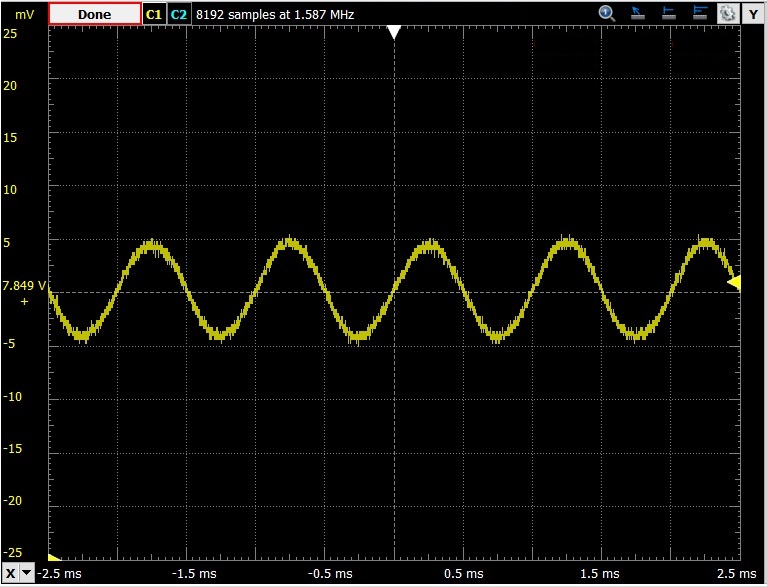
Non-Inverting and Inverting Inputs Tied Together Showing Common Mode Output
The following calculation provides the CMMR value of this differential amplifier:
Differential Mode Gain = OUT / (IN+ - IN-) = 1Vpp / (1Vpp - 0Vpp) = 1
Common Mode Gain = OUT / IN = 0.01Vpp / 1Vpp = 0.01
CMMR = Differential Mode Gain / Common Mode Gain = 1 / 0.01 = 100
CMMRdb = 20 * log (CMMR) = 40db
So this differential amplifier circuit is very simple, uses only one transistor, and can be scaled for various differential mode gains.
But...
It's CMMR isn't as good as a canonical diffamp or an OpAmp, and the input impedance on the non-inverting input is pretty low (around 1500 Ohms).
But if you take these into consideration it is easy to design a small amplifier that performs really well with just a few transistors.
Common Emitter Driver Stage
This is the voltage gain stage of the amplifier. Q2 amplifies the output of Q1 and provides +45db of voltage gain which is used to drive the push-pull output stage. To maximize gain and output voltage swing, Q2 doesn't use emitter degeneration so it's collector output will be fairly non-linear and temperature dependent. This is corrected with the DC feedback loop R7 and R8.
Collector current for Q2 is set at 5mA and flows through the speaker, R11, D1, and D2. This small current through the speaker isn't enough to generate measurable power or audible noise, but it provides a small feedback signal in the collector circuit of Q2 that corrects crossover distortion in Q3/Q4.
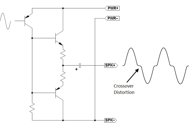
Crossover Distortion without Push-Pull Bias
The original amplifier circuit used a resistor to set the quiescent current for Q3/Q4. The voltage drop on that resistor was proportional to the collector current in Q2 and just slightly turned on Q3/Q4 so the amplifier would operate in a Class A mode for small signals. Unfortunately as the temperature changed in Q3/Q4, their base current would increase raising the voltage drop on the resistor. As the voltage drop on the resistor increased, the Q3/Q4 quiescent current would increase raising their temperature. This cycle would repeat until the temperatures of Q3/Q4 became so high they self destruct.
To avoid this, I've replaced the original resistor bias with D1 and D2. The combination of these two diodes provide a 1.4V bias for Q3/Q4 that is almost independent of the base current from Q3/Q4. Not exactly independent but much closer than a resistor. D1 and D2 also have a negative temperature coefficient with respect to junction voltage. So as the ambient temperature increases which tends to increase current in Q3/Q4, the junction voltage of D1/D2 decreases which reduces current in Q3/Q4. Ideally D1 and D2 should be physically close to Q3/Q4 (mounted on the heat sink if possible) but the diode stabilization circuit used here has worked extremely well in my temperature and output power tests. Capacitor C4 prevents ringing during Q3/Q4 crossover.
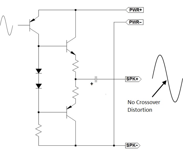
No Crossover Distortion with Push-Pull Diode Bias
Push-Pull Output Stage
The Push-Pull output stage provides the current gain needed in combination with the voltage gain of the CE Driver to produce the output power that drives the speaker. Q3 and Q4 work independently for large signals (Class B operation) but in tandem for small signals (Class A operation). For large signals, Q3 will conduct for one half of a cycle while Q4 will conduct for the other half. For small signals, Q3 and Q4 will contribute to both halves of the cycle.
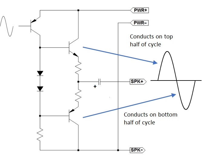
The DC output voltage on Q3/Q4 is 1/2 the power supply voltage in order to provide for the maximum AC voltage swing without clipping distortion. For a 9V battery, the Push-Pull DC output voltage is 4.5V. We don't want this DC voltage to appear on the speaker as that will waste a lot of power heating up the speaker coil and generating no sound in the process. We only want the AC voltage from the CE Driver stage to appear at the speaker. C5 decouples the DC output voltage on the Push-Pull stage from the speaker and allows only the AC voltage to appear. The trade-off with coupling capacitor C5 is that at low frequencies, the impedance of C5 will reduce the output voltage to the speaker which limits the lowest frequency from the music source that can be amplified which in this case is around 27 Hz.
The voltage gain of the Push-Pull output stage is -6db (loss) but the current gain for the Push-Pull stage is +35db which allows a tiny current in Q2 to produce a large current in Q3/Q4. The overall voltage gain of the amplifier is the sum of all the stage gains:
Diff Amp Gain + CE Driver Gain + Push-Pull Gain = (-21db) + 45db + (-6db) = +18db
Operating Parameters
After building the amplifier, the following operating parameters were measured with a power supply of 9V:
DC Quiescent Supply Current = 11mA per channel (22mA total)
Max Voltage Swing = 6Vpp
Power Supply Rejection = -20dB
Voltage Gain = +18db
Output Power at 1% THD = 0.525 W per channel
Input Impedance = 700 K Ohms
Frequency Response +/- 1db = 35 Hz to 20 KHz
Low Cutoff = 27 Hz
High Frequency Cutoff = 65 Khz
How to build the 8 Transistor Stereo Amplifier

The 8 Transistor Stereo Amplifier project described here is based on the Radio Shack pbox kit of the same name, but it has been updated with silicon transistors and passive components that can be easily obtained from electronics suppliers like Mouser and Digikey. I've built the redesigned amplifier kit described here and believe it works better than the original kit did back in 1969. To make it easy to replicate my work, I've provided illustrations and step-by-step assembly documentation based on the publication style used for the original product. But every page was created with original content specifically for the redesigned amplifier.
Download the Assembly Manual >>> HERE <<<.
I built the kit in two evenings, taking my time, and double-checking my progress while following the manual. If you are familiar with breadboard construction techniques, you can probably complete the project in a single evening.
Important Note:
Be sure to read through the "Tweaks and Hacks" section before you order parts and start building. You might want to include some of the suggested modifications during construction or dream up your own before you start.
Obtaining parts for the Stereo Amplifier project
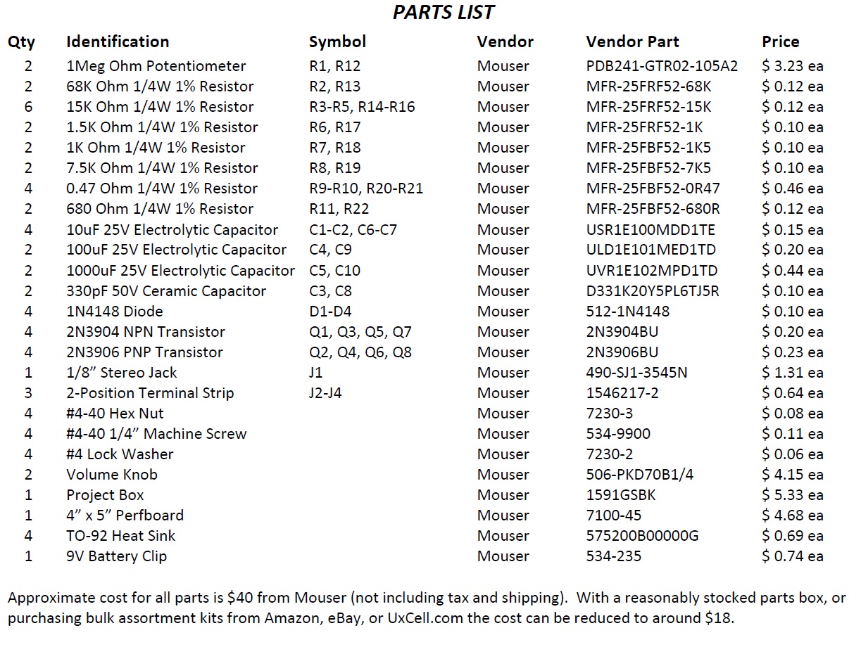
Review the parts list and obtain the components indicated. All components are available from Mouser or Digikey, or can be obtained from other suppliers that may be more convenient to your geography. Total cost for all new parts in small quantities is around $40 not including tax and shipping. To put that cost in perspective, the 8 Transistor Stereo Amplifier kit was introduced in 1969 at a retail price of $8.95. The economic value of $9 in 1969 is equivalent to around $61 today. If you deduct the cost of the volume knobs I've specified (knobs weren't included in the original kit) the amplifier project can be built for about half the adjusted cost of the project kit offered by Radio Shack in 1969. But keep in mind that Radio Shack needed to make a profit from the sale and support of their kit which explains the catalog price.
Below are a few notes regarding the parts used for the 8 Transistor Stereo Amplifier project:

NOTE: As of 2026, Joe Knows Electronics is no longer in business. I have left the content in place for historical purposes. There are many sellers on Amazon offering resistor assortments at great prices.
1. The resistors for the project can be purchased from Mouser, Digikey, Newark or other electronics component retailer. But I highly recommend the excellent Joe Knows Electronics resistor kit. It includes most (but not all) of the resistors you need for this project and over 860 different values that can be used for other projects, all labeled in individual plastic packages for $20. For this project I used all 1/4W resistors to save space. You can also find good deals on resistor kits from Amazon by searching for "resistor kit" and looking for a 1% tolerance kit that includes the most values and parts count for the best price. Some really good resistor kits can be found for less than $20. I've done that several times and have always been happy with the parts I received regardless of supplier.
2. The capacitors for the project can be purchased from Mouser, Digikey, Newark or other electronics component retailer. I used capacitors from the Joe Knows capacitor kit and an electrolytic assortment I found on Amazon for $10.
3. The transistors for the project are common 2N3904/2N3906 transistors that can be found just about anywhere by searching on the transistor number. All of the semiconductors I used came from the Joe Knows semiconductor kit. This is a great component assortment that comes with three booklets explaining how the components work and provides some example circuits to help illustrate how to hook them up in a circuit.
4. The case for the Stereo Amplifier project I built is a Hammond 1591GSBK ABS Project Box from Mouser. I used a piece of vector breadboard cut to fit on the top and spray painted with high temperature automotive flat red and finished with clear coat. I like the look of red on black, and the red color of the breadboard matched the red color of the original pbox kit. It's completely up to you how you want to house and color the kit you build.
5. The original pbox kit used tin-plated spring clips for attaching the battery, speakers, and input connections to the perf-board enclosure. These clips were a pain to solder to when new and they tarnished like crazy after they were installed resulting in intermittent connections. Fortunately for everyone they are no longer available. For this project I found that two position terminal strips and a 1/8" (3.5mm) stereo jack were a better solution.
Please Note: I have no business relationship with any of the above vendors. Nothing of financial value was exchanged for my recommendation. None of the above vendors provided compensation of any kind during the creation of this project. I will not be compensated in any way if you choose to build this project or purchase components from any vendor I recommend. I simply had a good experience with the vendors I recommend and believe you will too.
A bit of history associated with this project
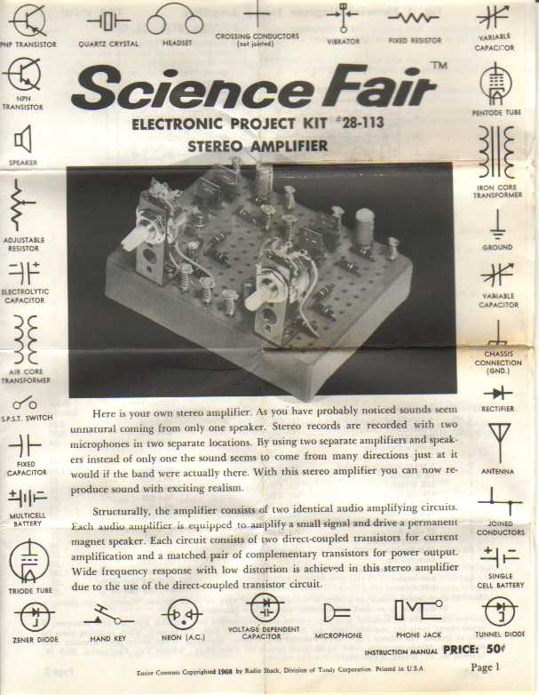
The original circuit design for the Stereo Amplifier from Radio Shack used 8 germanium transistors arranged in three stages: Differential Amplifier, CE Driver, and Push-Pull Output. These stages were common in high-end commercial amplifier design so the 8 Transistor Stereo Amplifier project should have earned a lot of fans back then. However, after only 3 years the kit was withdrawn which suggests that after the initial catalog marketing interval the product was only around for a year. When the kit was produced in 1969, Silicon junction transistors had replaced Germanium in new commercial amplifier designs. However, GE and ETCO continued selling Germanium transistors to hobbyists until about 1979 through Radio Shack, Lafayette, Poly Paks, and others. So, why did the kit not have a successful run?
Well, there are some good reasons:
Germanium was a relatively easy element to work with during the early days of the transistor but it's weaknesses made Silicon a more attractive element after manufacturing challenges were overcome. Germanium has a lower energy gap between the valence and conduction band which results in higher leakage current proportional to temperature. Germanium has lower thermal conductivity than silicon which makes it harder for the transistor get rid of internally generated heat. As internal temperature rises, more leakage current occurs which generates more heat... and so on. These two properties combined can result in thermal runaway ending in device self destruction. The original amplifier design did not provide a method for preventing thermal runaway in a push-pull configuration which made the amplifier unreliable.
By 1959 no manufacturer had discovered a way to build an oxide on Germanium. This allowed Silicon oxide planar transistors to achieve manufacturing dominance in terms of yield, cost, and reliability. As the cost of Silicon transistors fell, Germanium could not keep up and eventually the transistors used in the kit became too expensive. To minimize the potential for thermal runaway, Radio Shack sold matched pair semiconductors that were sorted by hand which further increased the cost of the transistors.
At $9.00 ($61 in 2017) the 8 Transistor Stereo Amplifier was the most expensive kit in the Pbox line and contained 56 parts. By comparison the 3 Transistor Short Wave Radio kit at $8 had only 39 parts and the FM Wireless Microphone kit at $7 had only 23. I suspect there were very few young customers able to afford a product this complex, and there were more factory rework and refund returns than anticipated.
So...
To overcome the limitations of the original kit, I've included a few modifications to improve performance and reliability including:
1. Redesign the amplifier to use readily available Silicon transistors.
2. Improved bias control for push-pull stage.
3. Increase output coupling capacitance to improve low frequency response.
4. Add compensation capacitor to increase high frequency roll-off above audio frequencies.
5. Replace tin-plated spring terminals with terminal strips and stereo jack to improve connection reliability.
6. Re-scale amplifier gain for maximum power at modern line level voltages.
I haven't attempted to simplify the project. My redesign requires 69 parts and the assembly document is 9 pages long. So I do not recommend this project for a novice. But if you like working with discrete analog components on perfboard and you have good soldering skills, this project is just the right challenge.
I think this kit redesign is far and away the most fun I've had working on these Pbox redesigns. The 8 Transistor Stereo Amplifier project I built can easily fill a room with great sound when attached to a set of good speakers. It's impressive what can be achieved with a few transistors and a standard 9V battery (even if that battery won't last long at full power).
Review the circuit board layout
Circuit Board Layout (Top)
The Assembly Manual provides a step-by-step checklist for installing and soldering each component to the pefboard. As you can see from the opposite side illustration, I've used point-to-point wiring with 24 AWG solid hookup wire. Most of the connections can be made with just the component leads. But power, ground, and signal bus leads are best done with lengths of hookup wire.
Circuit Board Layout (Bottom)
When it comes to wiring, try to be as neat as I've indicated in the assembly manual. You don't have to be the world's best soldering artist but there's no good reason to do the work half-way. Go all out and make your project look as good as you can.
Preparing the perfboard before mounting components
The perfboard specified in the parts list is too large to fit onto the Hammond case so some trimming is required as indicated in the images below. Follow the steps below to prepare the perfboard before installing components:
Warning: When I write, "sharp edge" I mean Xacto knife or similar. Those products are extremely sharp (think surgical scalpel) and can do a lot of damage if you aren't extremely careful. Use extreme care when operating any cutting tool.
1. Using a sharp edge, carefully score the perfboard along the TOP ROW and BOTTOM ROW row of holes all the way to the end of the board. Run the sharp edge over the score line several times until it penetrates 1/4 to 1/2 way through the perfboard.
2. Using a sharp edge, carefully score the perfboard along the RIGHT COLUMN and LEFT COLUMN of holes all the way to the end of the board. Run the sharp edge over the score line several times until it penetrates 1/4 to 1/2 way through the perfboard.
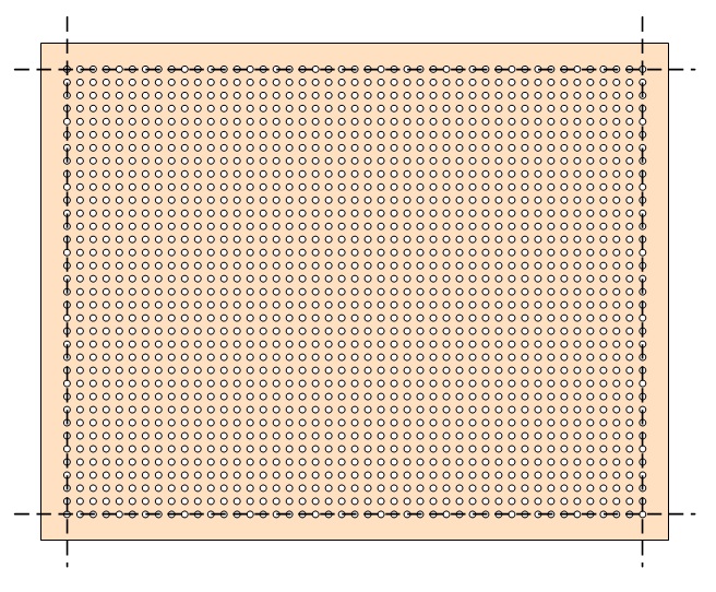
Score edges of perfboard along dashed lines
3. Using a small pair of pliers, carefully bend the TOP ROW section back away from the score line. Work with one end of the TOP ROW, moving to the center, and then the other end. The TOP ROW section will eventually break away from the perfboard.
4. Using a small pair of pliers, carefully bend the BOTTOM ROW section back away from the score line. Work with one end of the BOTTOM ROW, moving to the center, and then the other end. The BOTTOM ROW section will eventually break away from the perfboard.
5. Using a small pair of pliers, carefully bend the RIGHT COLUMN section back away from the score line. Work with one end of the RIGHT COLUMN, moving to the center, and then the other end. The RIGHT COLUMN section will eventually break away from the perfboard.
6. Using a small pair of pliers, carefully bend the LEFT COLUMN section back away from the score line. Work with one end of the LEFT COLUMN, moving to the center, and then the other end. The COLUMN section will eventually break away from the perfboard.

Carefully break apart perfboard edges along score lines
7. Using an Exacto knife, match the trimmed perfboard with the Hammond case and enlarge holes at the corner to match with the corner mounting holes in the case. Work slowly and carefully with minimal pressure to avoid breaking the corner piece.
8. Place the potentiometer mounting brackets onto the perfboard and enlarge holes in the perfboard to match the holes in the brackets. Work slowly and carefully with minimal pressure to avoid cracking the perfboard.

Cut holes for case and bracket screws
9. Spray paint the perfboard with the color of your choice or leave it natural. It's your choice.

Paint with desired color
I typically use flat red followed up with 2 to 3 coats of gloss clear.
Fabricate and mount the volume control brackets
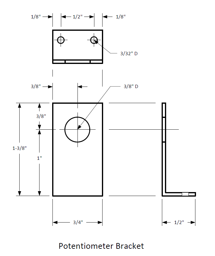
The volume control brackets I made were from an old license plate that I cut with tin snips. But you can use any thin metal you have available. I've used PCI slot covers from an old desktop computer to good effect as well. I spray painted the brackets with a dark grey automotive paint but you can use any color that looks cool to you. There is no try. Do, or do not.
Follow the first few steps in the assembly manual to install the volume control mounting brackets. When completed, the project should look something like the images below.
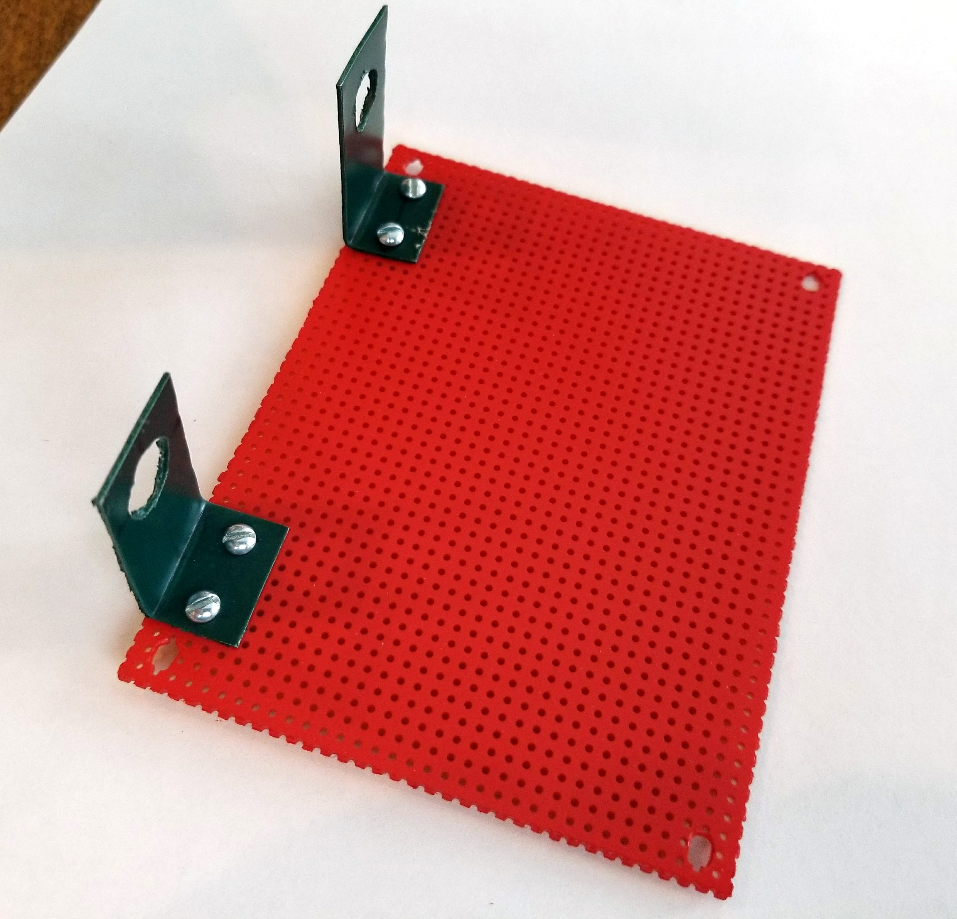
Mount the Volume Controls
The potentiometers specified in the parts list come with hex nuts and flat washers. The assembly manual shows the order in which to install this hardware. So that the potentiometer shaft does not extend out too far from the bracket, I installed the inside hex nut and flat washer so that the outside hex nut and washer would sit just inside the first couple of threads on the shaft.
Important Note: If you use a different vendor for the potentiometers than I've specified, make sure they ship with mounting hardware or you will need to purchase your own.

The potentiometers and their mounting hardware
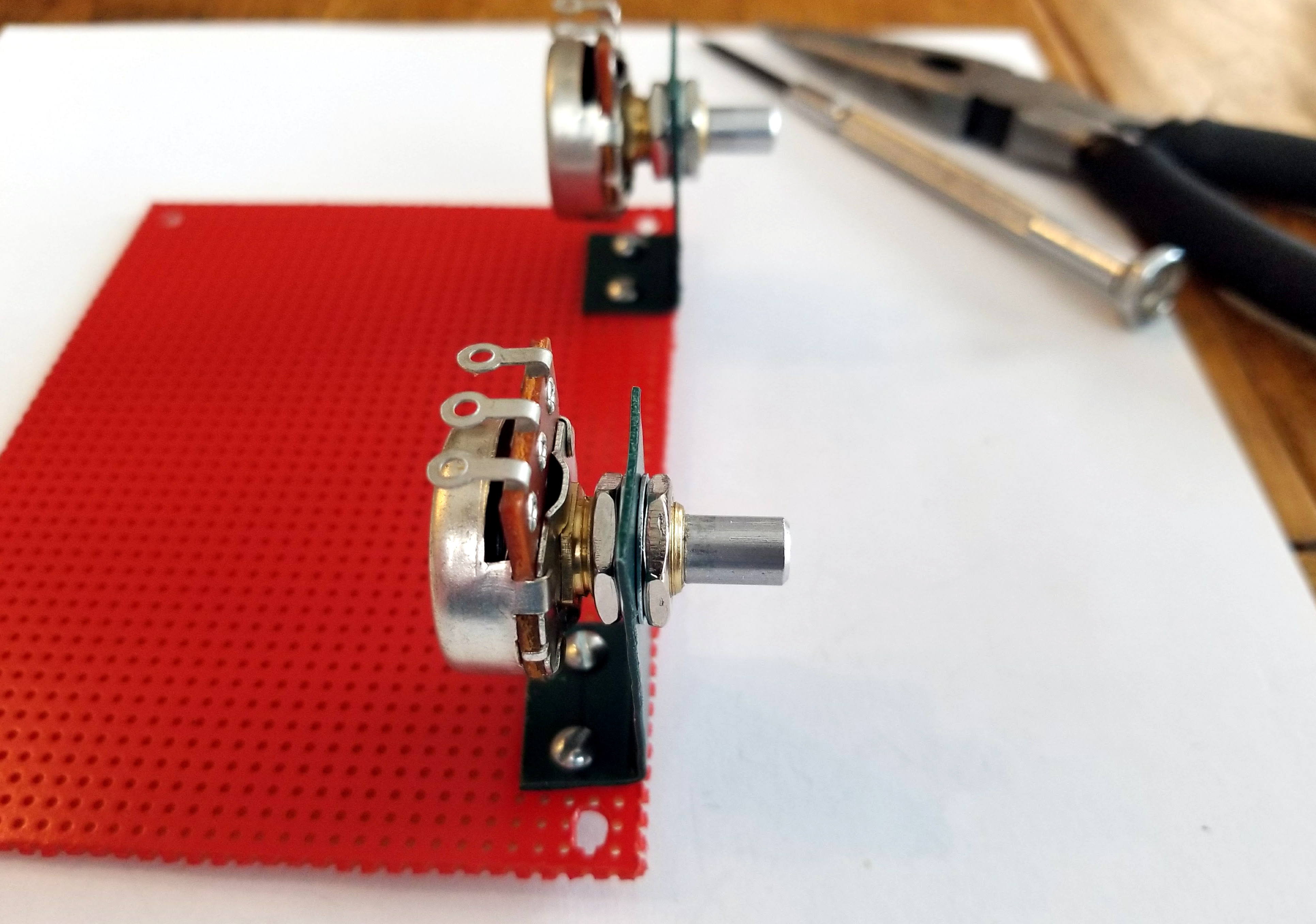
Position of mounting hardware on the bracket
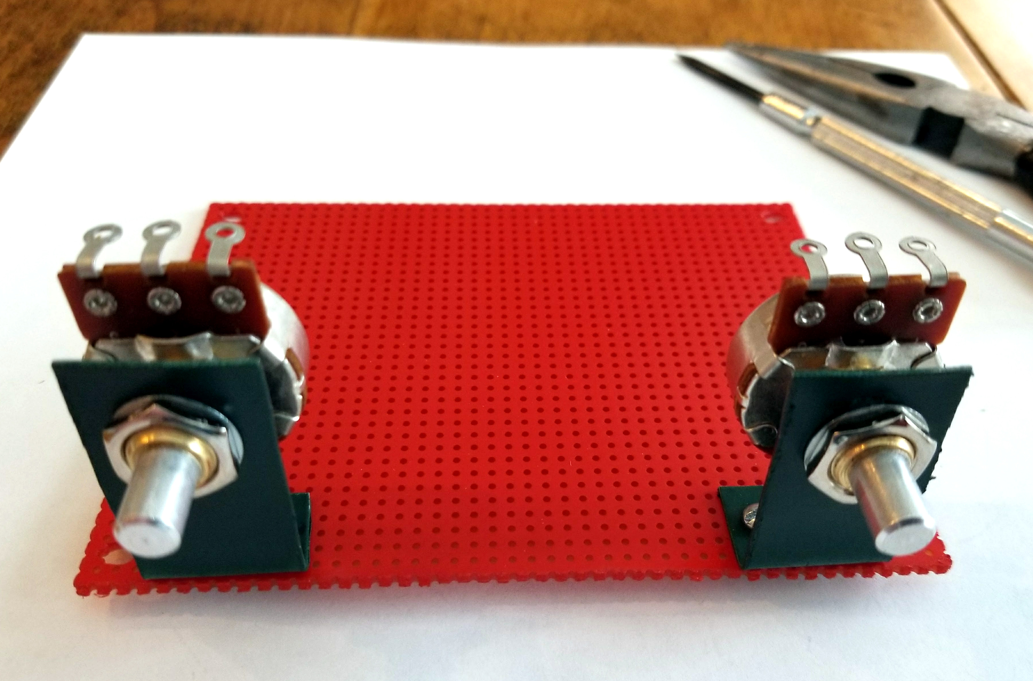
Potentiometers and hardware installed
Install input, speaker, and power connectors
The 1/8" (3.5mm) stereo jack specified in the parts list comes with pins pre-formed for automatic insertion into a PCB board. I straightened the pins out with pliers, lined up the pins on the perfboard, and firmly pressed down on the connector to seat it flush. You may need to slightly enlarge the perfboard holes if the connector will not seat with moderate force. Do not apply excessive pressure.
The three 2-position terminal strips will sit flush on the perfboard with very little force. Bend the pins slightly outward to keep them in place.
The assembly manual covers these steps, but I wanted you to be able to see what the board should look like when all connectors are installed.
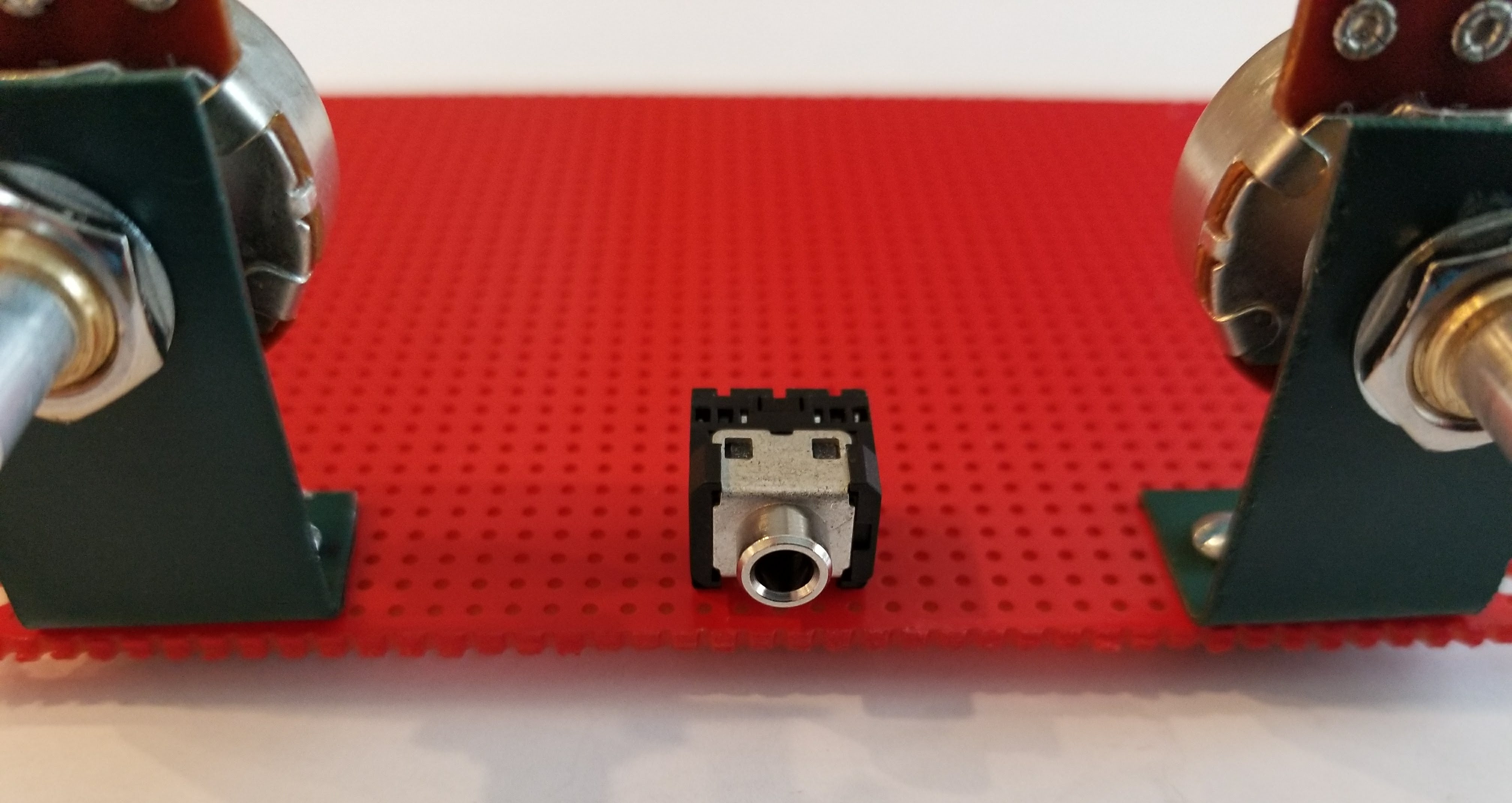
Stereo Jack Installed
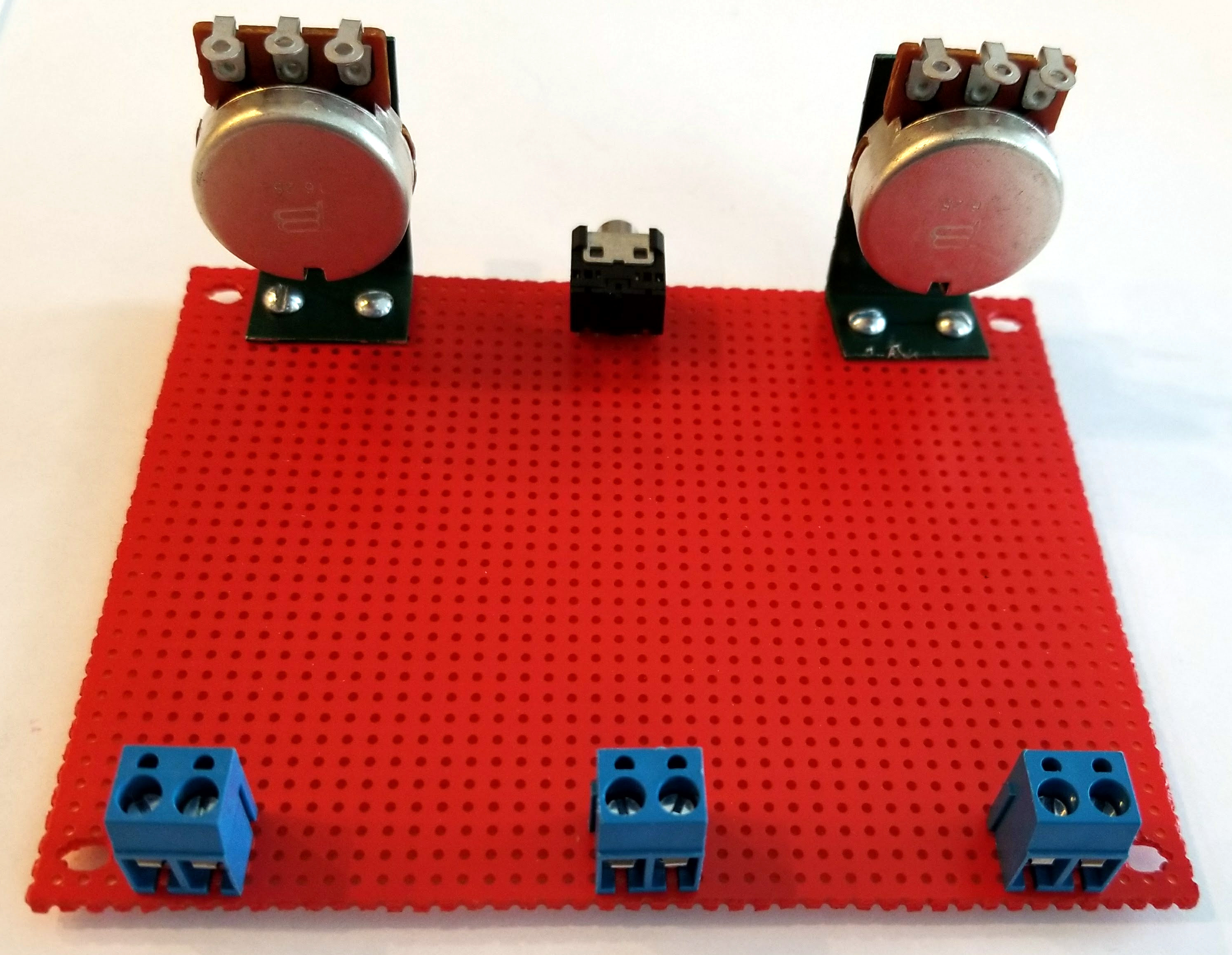
Speaker and Power Connectors Installed
Assembly Photos: Completed Left Channel
When completed, the left channel amplifier should look something like the images below. I used colored hookup wire for the potentiometer connections so it would be easier to identify each potentiometer lug (A, B, or C).
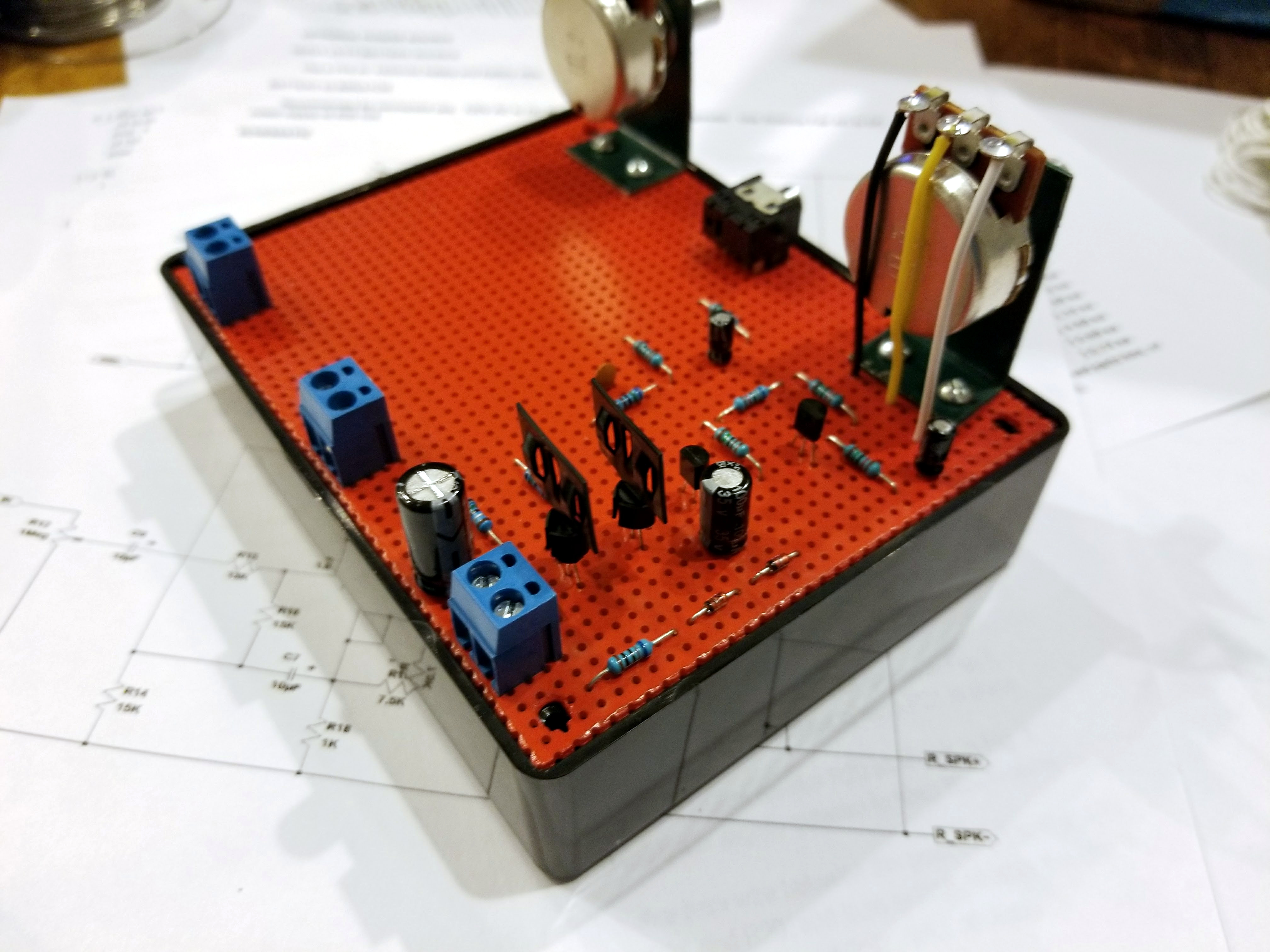
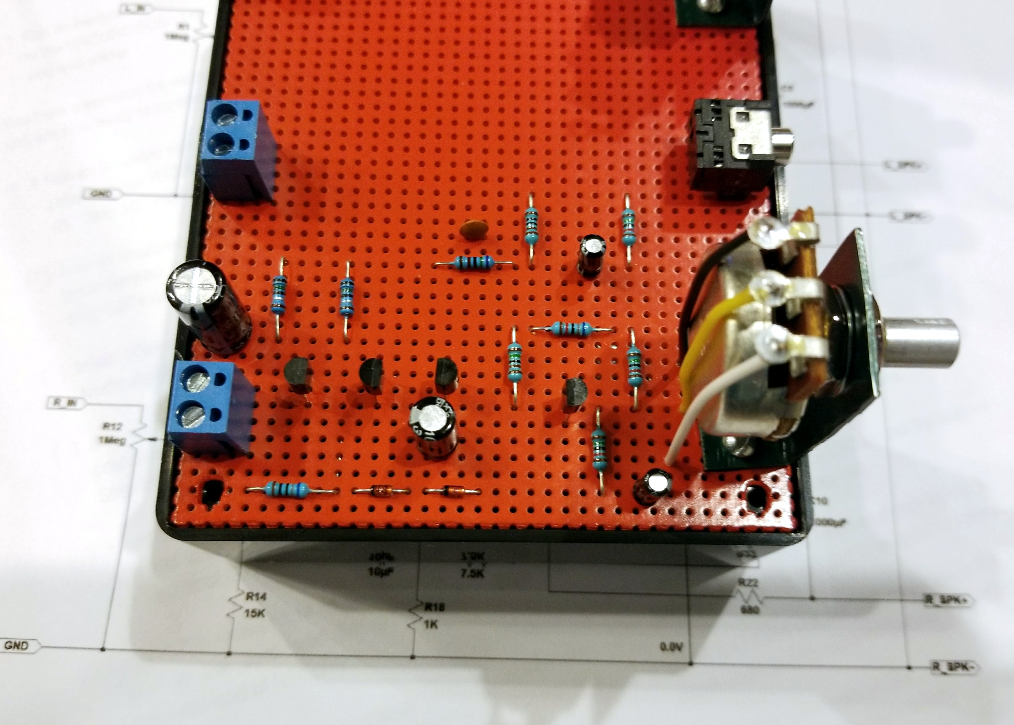
Assembly Photos: Completed Right Channel
When completed, the right channel amplifier should look something like the images below. I used colored hookup wire for the potentiometer connections so it would be easier to identify each potentiometer lug (A, B, or C).
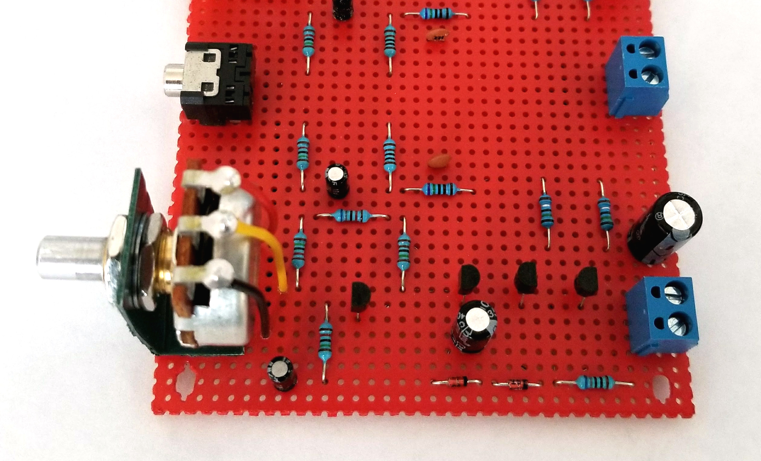
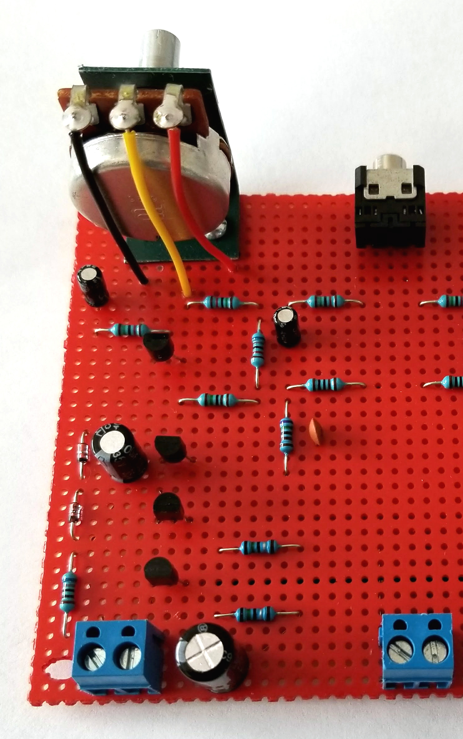
Assembly Photos: Completed Stereo Channel
When completed, the 8 Transistor Stereo Amplifier should look something like the images below. You are now ready to attach the battery and speakers, plug in a sound source, and listen to some tunes on an amp you built yourself.
The assembly manual covers the setup and operation of the amplifier along with some modifications you can make to double the output power if desired. Although for me, 1W was impressive enough.
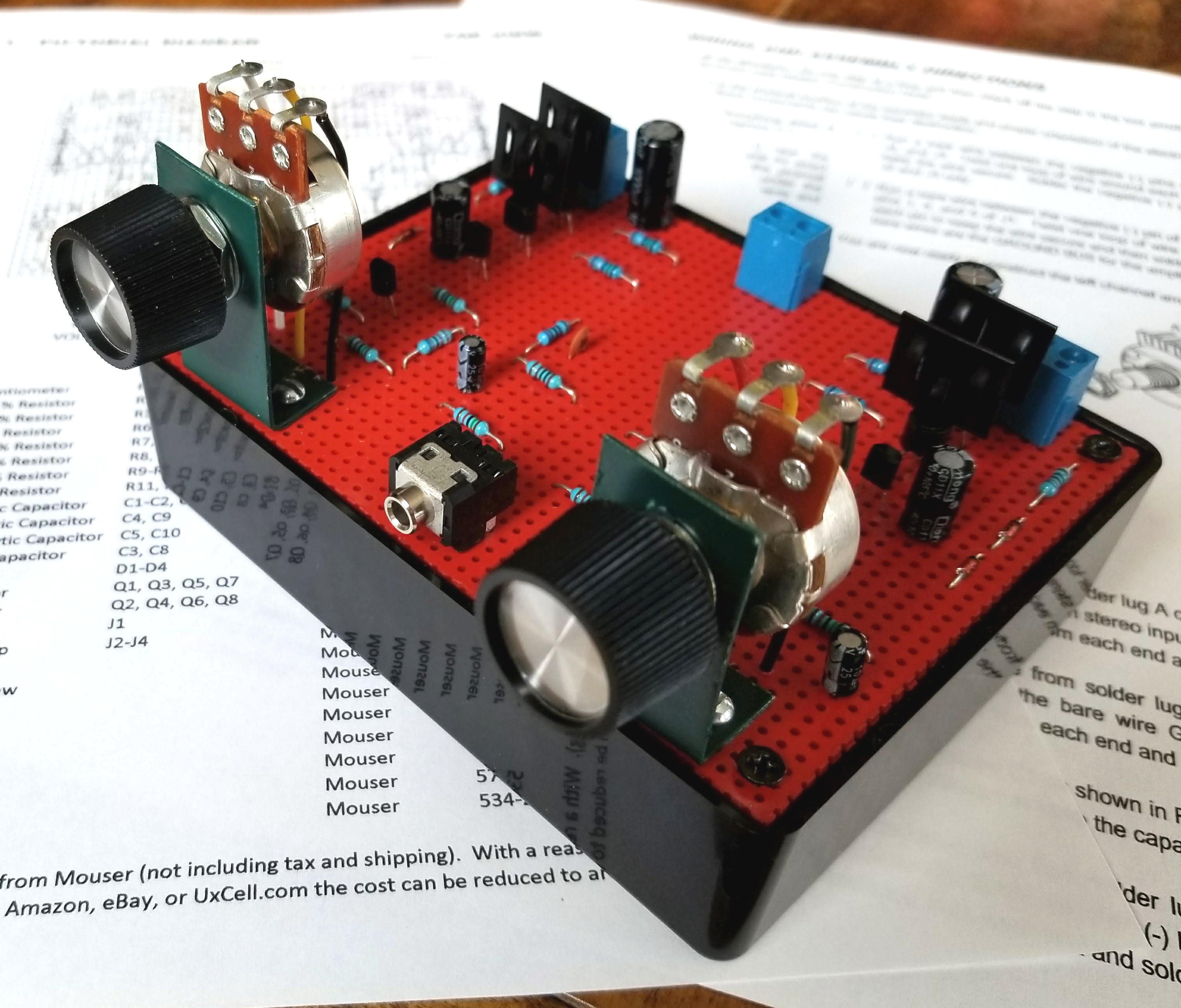
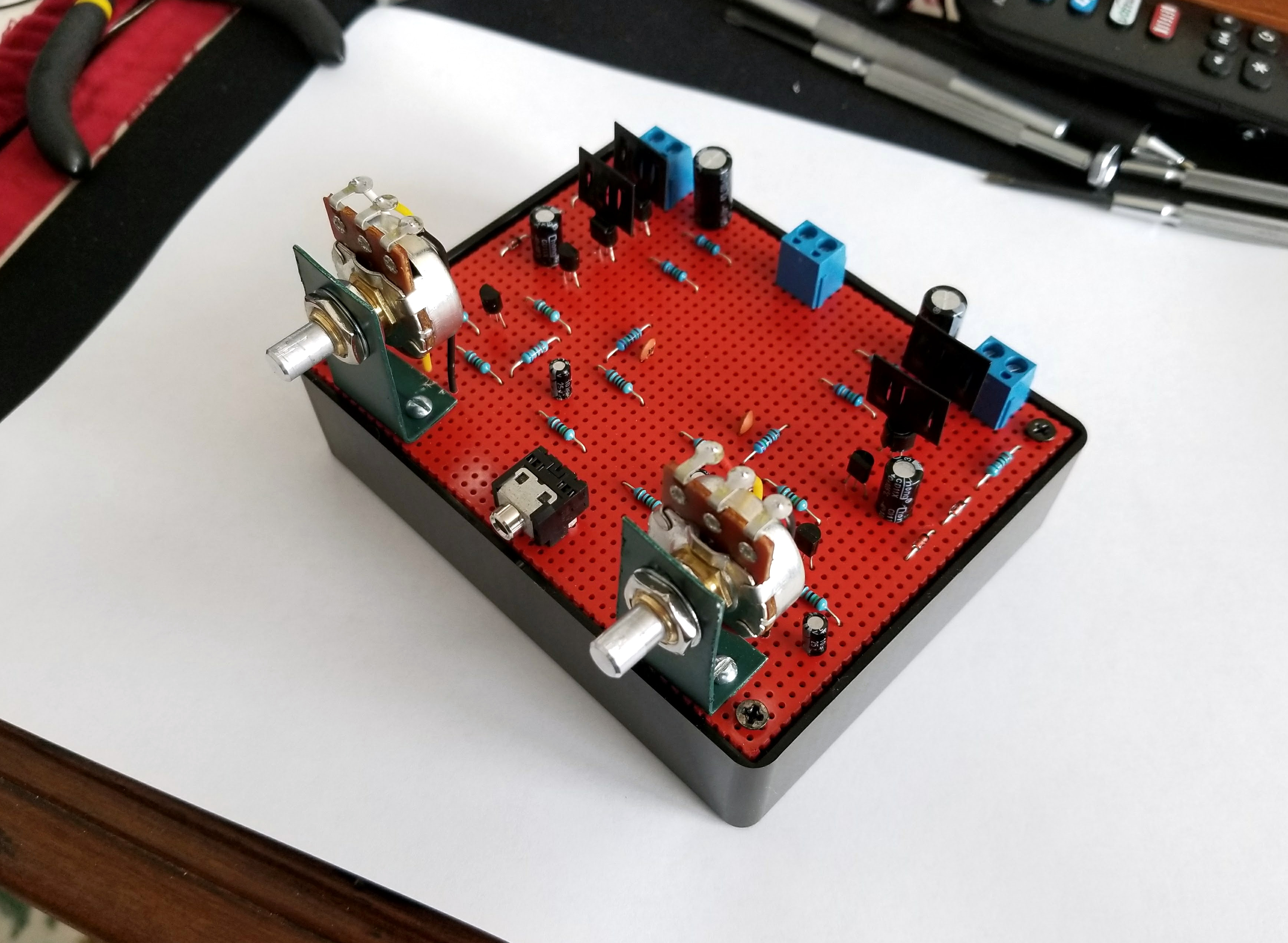
If hope you enjoyed this article. Thanks for reading!
NetZener