I'm working on a project that requires a portable battery-fed power supply that provides variable output voltage and an adjustable current limit. I needed an output voltage between 0 and 12V, current limit between 10mA and 1A, and load regulation 0.1% or better at full output voltage and current. Because the supply would be used in noise sensitive analog circuit design, I couldn't use one of the many switching regulator options available due to the 100mV of high frequency noise that's typical of those products.
The well-known LM317 is an easy way to meet my variable voltage requirement but constant current control isn't its strength. And its minimum output voltage is around 1.25V. Not a major issue but I would prefer to be able to drop the supply voltage to 0V when needed instead of having to flip a switch.
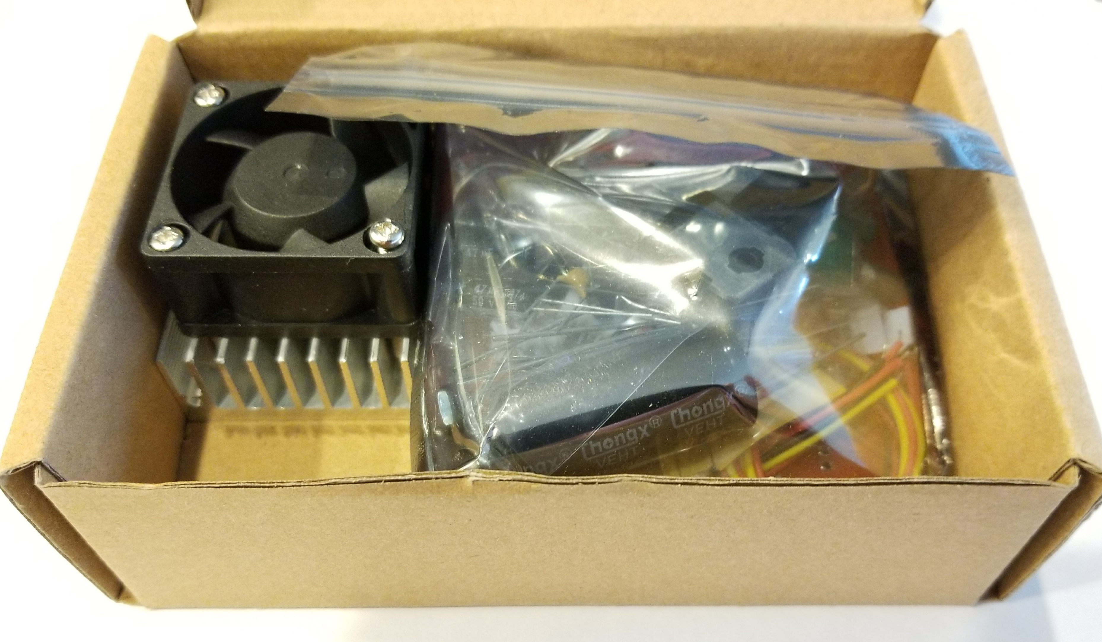
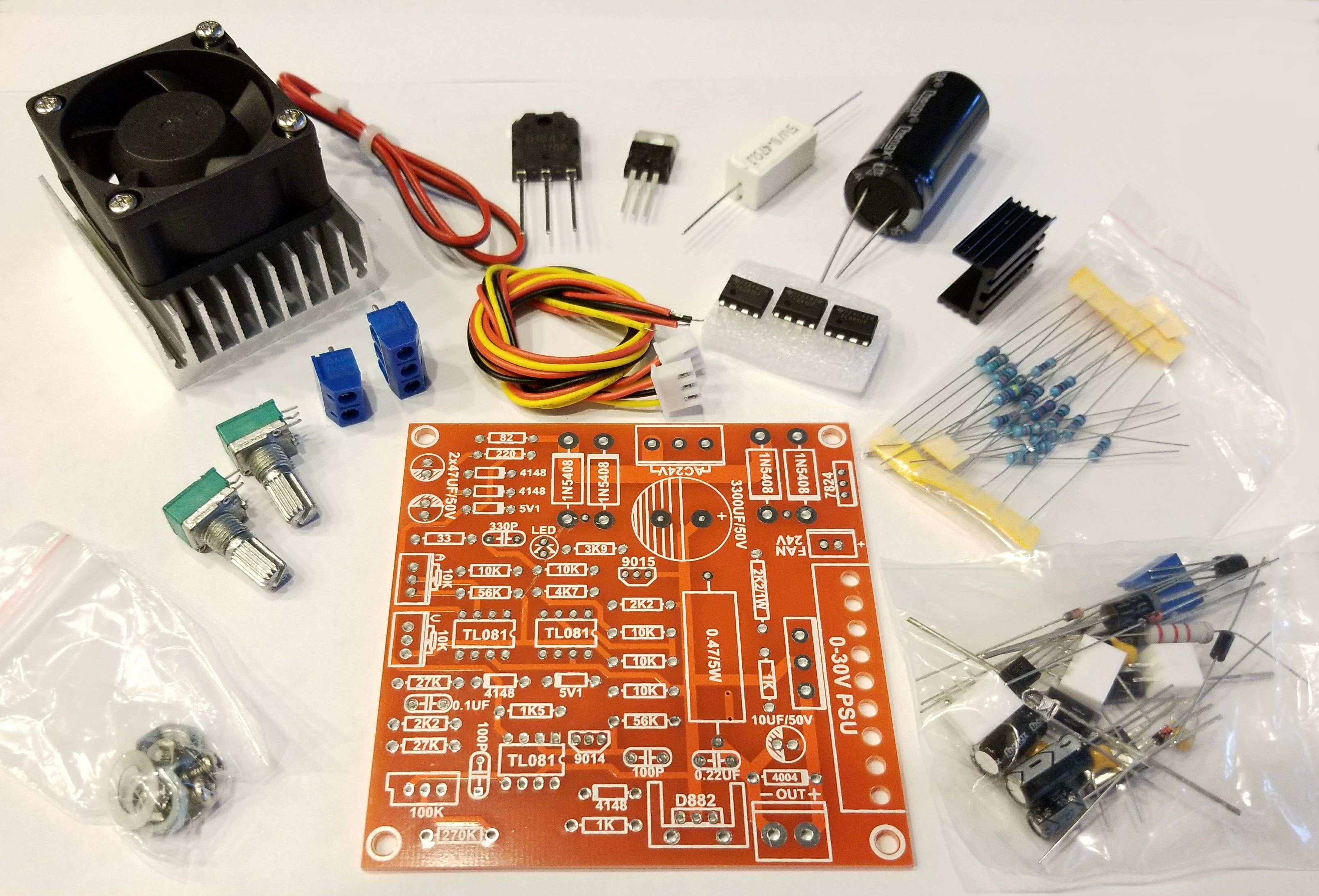
Before starting a custom design I thought I'd see what was available off-the-shelf, preferably in a DIY kit form so I would have some options on component values and controls placement. One product that consistently appeared on Amazon and eBay was the power supply kit featured in this article. The cost of the kit was so cheap I ordered two without doing further research. After receiving the kit I was impressed with the quality of the packaging, circuit board, and the variety of components included. Whatever the outcome, this kit was definitely worth the price.
After reviewing the documentation available on the Internet, the following phrase in bold letters caused some concern: "The circuit must be connected to 24V alternating current power, and direct current is forbidden". A quick look at the schematic told me why. The current limiter, error amplifier, and current pass depends on an -5V auxiliary supply derived from the main bridge rectifier. After thinking about the problem a few minutes the solution was obvious and is covered in Part 2 of this article. I've found an analog variable power supply kit that, with some modifications, fit my requirement exactly.
Introduction to the WeiKedz Variable Power Supply DIY Kit
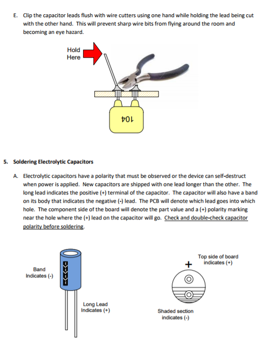
Introduction
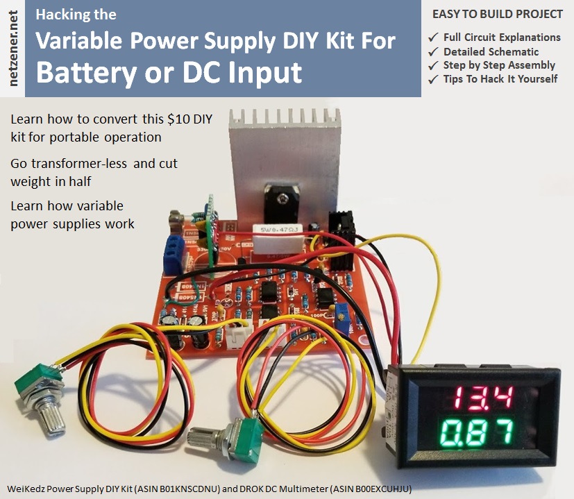
The WeiKedz Variable Power Supply DIY kit is an electronics project kit containing all the components needed to build an analog variable power supply EXCEPT transformer, power cord, knobs, and enclosure (more on this later). There are a number of distributors in Asia offering this kit under various brand names. But as of November, 2017 the WeiKedz branded version was available on Amazon (ASIN B01KNSCDNU) with Prime shipping for $14, which in my opinion is a great value considering WeiKidz includes a large aluminum heat sink, 24V fan, and mounting hardware.
The specifications for the power supply are as follows:
Input voltage: 24VAC
Input current: 3A (maximum)
Output voltage: 0-30VDC (adjustable)
Output current: 2mA to 3A (adjustable)
Output voltage ripple: maximum 0.01%
As you will see in the analysis sections that follow, these specifications are too optimistic. The power supply I assembled works very well and is suitable for almost any analog project the beginner or experienced maker is likely to find exciting. But it is not, by design, capable of achieving exactly these specifications. In addition, I ended up substituting a 20VAC transformer (Hammond 185F20) for the 24VAC transformer specified in the documentation in order to keep OpAmp supply voltages below the manufacturers maximum ratings. There is some assembly documentation available on the Internet, but it is hard to find and has some technical and English language weaknesses that I've corrected in the assembly document attached below. That being said, for $14 and the cost of a transformer it's a great kit that is fun to build. A V/I multimeter can be added to make it easier to set the output voltage and current limit.
Parts List and Component Identifier
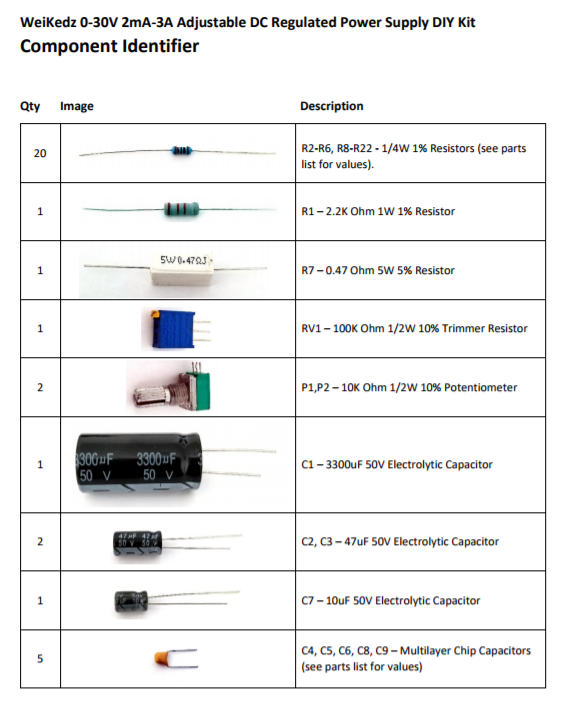
Attached below are the parts list and component identifier documents describing everything that came with my kit. For those new to electronics, the component identifier document will help you figure out which part is which. For some reason the manufacturers web site shows components that look like somebody stuffed them in their jeans and accidentally ran them through the wash. Never fear, all of the parts I received were well packed, protected where needed, and with clean and straight leads. So yours should arrive that way too.
Download the Parts List document >>> HERE <<<
Download the Component Identifier document >>> HERE <<<
Assembly Manual
If you should decide to build the WeiKedz power supply, I've also included a comprehensive assembly guide below that is a bit more detailed than that provided by the manufacturer. If you are new to electronics but have some experience with a soldering iron, this guide will provide just about everything you need to know to successfully build the kit.
Download the Assembly Manual >>> HERE <<<
Operation and Maintenance Guide
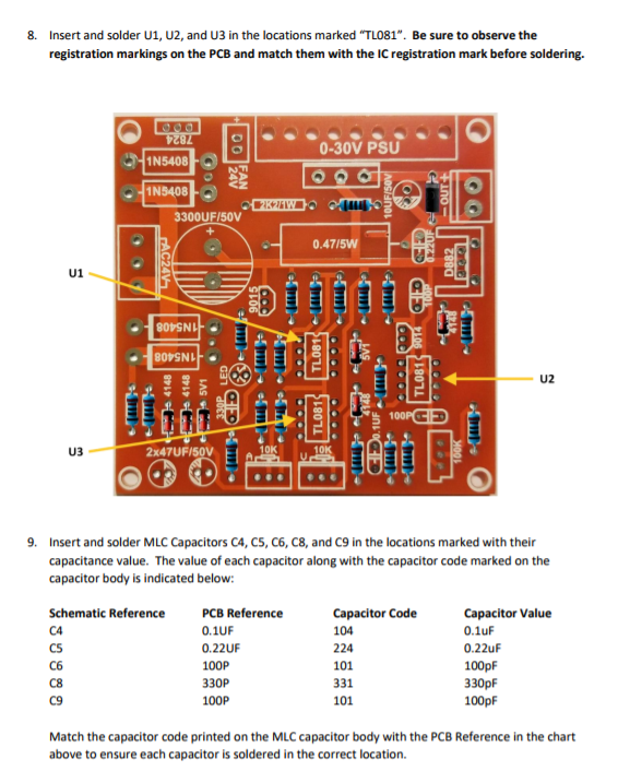
One of the weaknesses in the manufacturing design of the circuit board was the decision to use component values (100K, 4004, 5V1, etc.) on the component layer silk screen instead of schematic reference numbers (R1, C2, Q4, etc). The decision to use component values helps an experienced builder solder parts to the board with minimal documentation. But if you ever need to troubleshoot the power supply using the circuit diagram you are out of luck. The lack of reference numbers on the board makes matching a node on the schematic with the corresponding node on the circuit board very, very difficult. For example, there are five 10K Ohm resistors on the circuit board. Without a schematic reference number on the board, you can't tell which 10K resistor on the board goes with which 10K Ohm resistor on the schematic. All of the documentation I've included uses both component values and schematic references. The Operation and Maintenance guide contains images of the board along with it's components, component values, and schematic reference numbers. It also contains the tune-up procedures and some troubleshooting steps to follow if the power supply doesn't work properly. You will find this guide invaluable to maintaining the power supply.
Download the Operations and Maintenance Guide >>> HERE <<<
Circuit Analysis
In the next few sections, I'll break the power supply schematic down into it's major functional blocks and describe how each works and what most of the components do. This will help in determining how to make changes and substitutions that tailor the power supply for a specific application. For example, WeiKedz and other brands offering this kit for sale are not very specific on the transformer needed, which has been a source of most of the confusion builders have had with the kit. I'll clear that right up and show you how to make the proper selection based on your voltage and current requirements.
Hacking It
At the end of this article, I'll describe the changes needed to convert the power supply to portable (i.e. battery) operation and add a V/I display. This is the version shown on the cover. As you will see later, it's not as simple as attaching a battery with the correct voltage.
A note on content
Where possible I've attempted to describe the operation of various circuits using basic mathematics. The majority of electronic design can be done with a good understanding of algebra and a little bit of trigonometry (occasionally pressing the sin or cos button). Electronics concepts and some experience with the usual fundamental equations like Ohms Law, RC time constants, power factor, etc. is necessary. But I'm more interested in communicating the importance of one skill in particular: The ability to observe a physical system in action, write an equation that describes what is being observed, and use that equation to predict what will happen when the system is changed. THAT is a far more useful skill than just memorizing the laws of exponents. Designing and then building a working circuit is way more fun and satisfying than blindly plugging in one resistor or capacitor value after another until it works. I know some folks who are pretty good at doing things that way, but they are more interested in the art of the thing than the science.
Special Note: I have no business relationship with any vendor mentioned in this article. Nothing of financial value was exchanged for my recommendation. None of the vendors mentioned in this article provided compensation of any kind during the creation of this project. I will not be compensated in any way if you choose to build this project or purchase components from any vendor I recommend. I simply had a good experience with the vendors I recommend and believe you will too.
Power Supply Block Diagram and Schematic Diagram
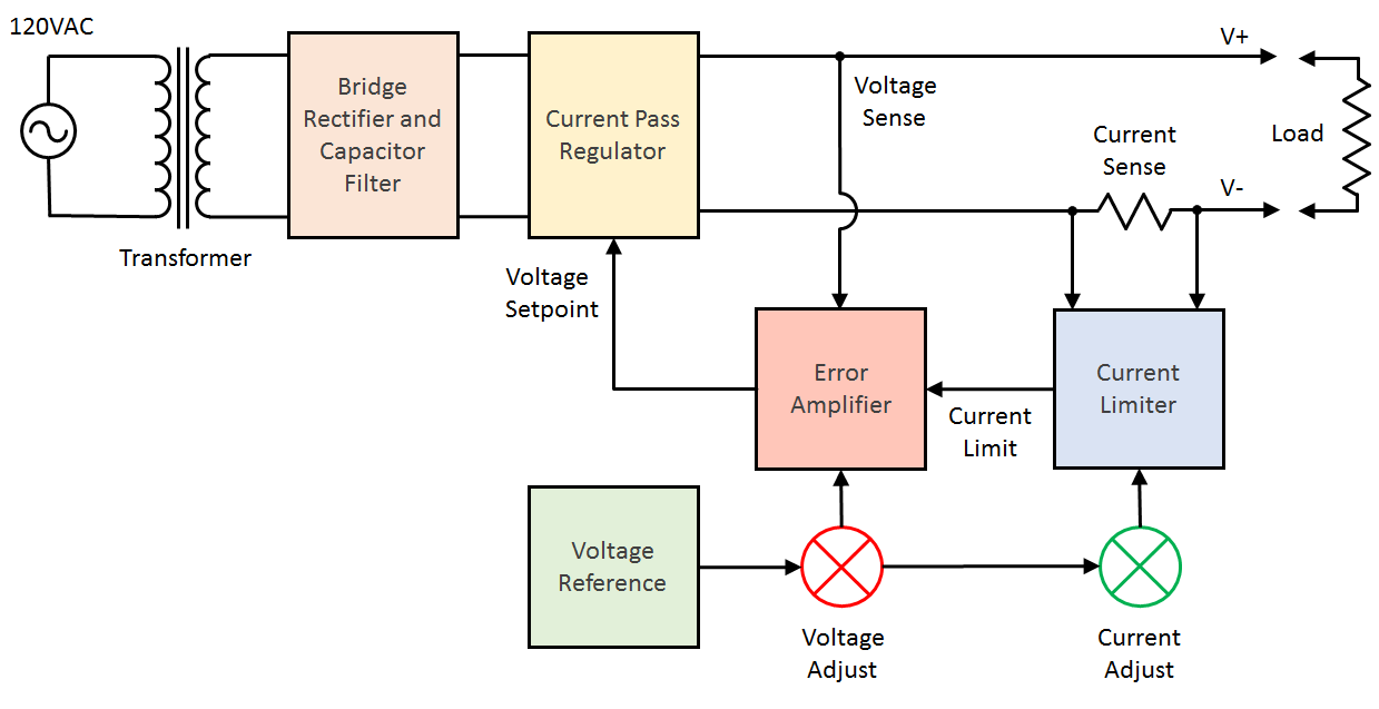
The WeiKedz variable power supply is a fairly standard design with 5 functional blocks as described below:
Bridge Rectifier and Capacitor Filter
Converts the 24 VAC power from the transformer into +32.5 VDC and -5 VDC power for use by other function blocks.
Voltage Reference
This is the heart of the power supply. It's job is to provide a fixed known reference voltage that other function blocks use to control the power supply output voltage and limit the power supply output current.
Error Amplifier
This function works much like the thermostat in your home. You set the temperature you want, the thermostat compares that to the actual indoor temperature, and then signals the climate control system raise or lower the indoor temperature to match. The error amplifier works the same way. You set the output voltage you want, the error amplifier compares that to the actual output voltage and signals the Current Pass function to raise or lower the output voltage to match.
Current Limiter
This function works in similar fashion to the Error Amplifier except that it senses the output current (as opposed to the output voltage) and signals the Error Amplifier to reduce the output voltage when the current limit is exceeded. This helps prevent damage to the components of a circuit caused by wiring or design error.
Current Pass Regulator
This is the workhorse of the power supply. It's job is to maintain the voltage set by the Error Amplifier independent of the current drawn by the circuit attached to the power supply. During normal operation the power consumed by the circuit attached to the power supply will be less than the output power of the Bridge Rectifier/Filter function. This difference in power has to be consumed by the Current Pass Regulator and released as heat, which is why this function has large metal heat sinks attached.
Summary
I've attached a PDF version of the schematic for the WeiKedz variable power supply below along with the voltages that will appear when a 24 VAC transformer is attached. Each of the function blocks above is described in detail in the steps that follow.
Download the Power Supply Schematic >>> HERE <<<
Problems With the WeiKedz Power Supply Design
Before I start the analysis I'd like to mention that the manufacturers specifications for the power supply are far too aggressive.
This is not a power supply capable of reliably delivering 0-30VDC at 0-3A. The power supply I assembled was unable to achieve the manufacturers specifications for all voltage and currents. For example, I experienced overheating in capacitor C1 and transistor Q4 when drawing 3 Amps from a 5V output setting which would have resulted in the catastrophic failure of these components had I allowed the test to run uninterrupted. You'll see why in the sections that follow.
Below is the short list of issues with the design:
1. Transformer VI recommendation is under-sized.
2. Ripple current for C1 exceeds manufacturers maximum ratings when output current >1A.
3. Power supply range (V+ and V-) exceeds manufacturers maximum ratings for U2 and U3 (TL081).
4. Vceo for Q2 (2SD882) exceeds manufacturers maximum rating when output voltage is 0.
5. Ripple voltage for C1 exceeds regulation window for 30V at output current >100mA
The above issues will result in near-term component failure after the power supply is placed in service.
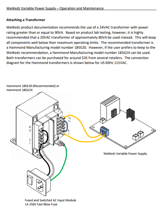
However, I think the power supply is a good design that has simply been over-specified. Below are my recommendations for how the power supply should be operated for good long-term reliability if no component substitutions are made:
Transformer: 20V RMS @ 4A (Hammond 185E20)
Output Voltage: 0-20V
Output Current: 0-1A
With the above ratings, the fan can be omitted and the large heat sink on Q4 can be reduced in size (I cut mine almost in half). The transformer sizing I've specified covers you for the low power factor of the secondary current and allows for +/- 10% line voltage tolerance at the mains. And, the full 1A current can be drawn from any output voltage setting.
1. Analysis - Rectifier and Filter Circuit
If you examine the schematic diagram above, you will notice that there are three power supplies associated with this function block: The V+ Supply, the V- Supply, and the Fan Supply. A short description of each is provided below followed by a more detailed operating analysis.
Description: The V+ Supply
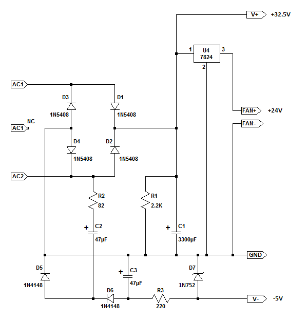
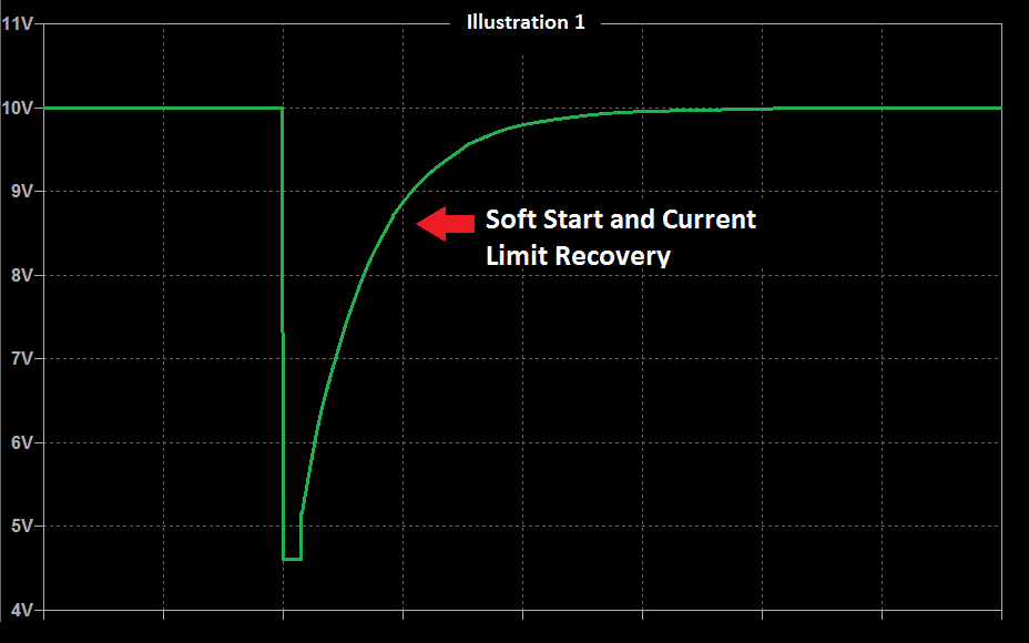
The rectifier and filter section is a very basic full-wave bridge circuit (D1 through D4) with a large filter capacitor attached (C1). Resistor R1 will safely discharge C1 when AC power is disconnected from the transformer. Regulator U4 drops the V+ voltage to 24V to power the cooling fan provided in the kit. The transformer attached to the power supply provides an alternating current (AC) voltage with frequency of 50Hz or 60Hz depending on country. On the positive half of the AC cycle, diodes D1 and D4 conduct which charges capacitor C1 for that portion of the cycle. On the negative half of the AC cycle, diodes D2 and D3 conduct which also charges capacitor C1 for that portion of the cycle. See Illustration 1 below.
Description: The V- Supply
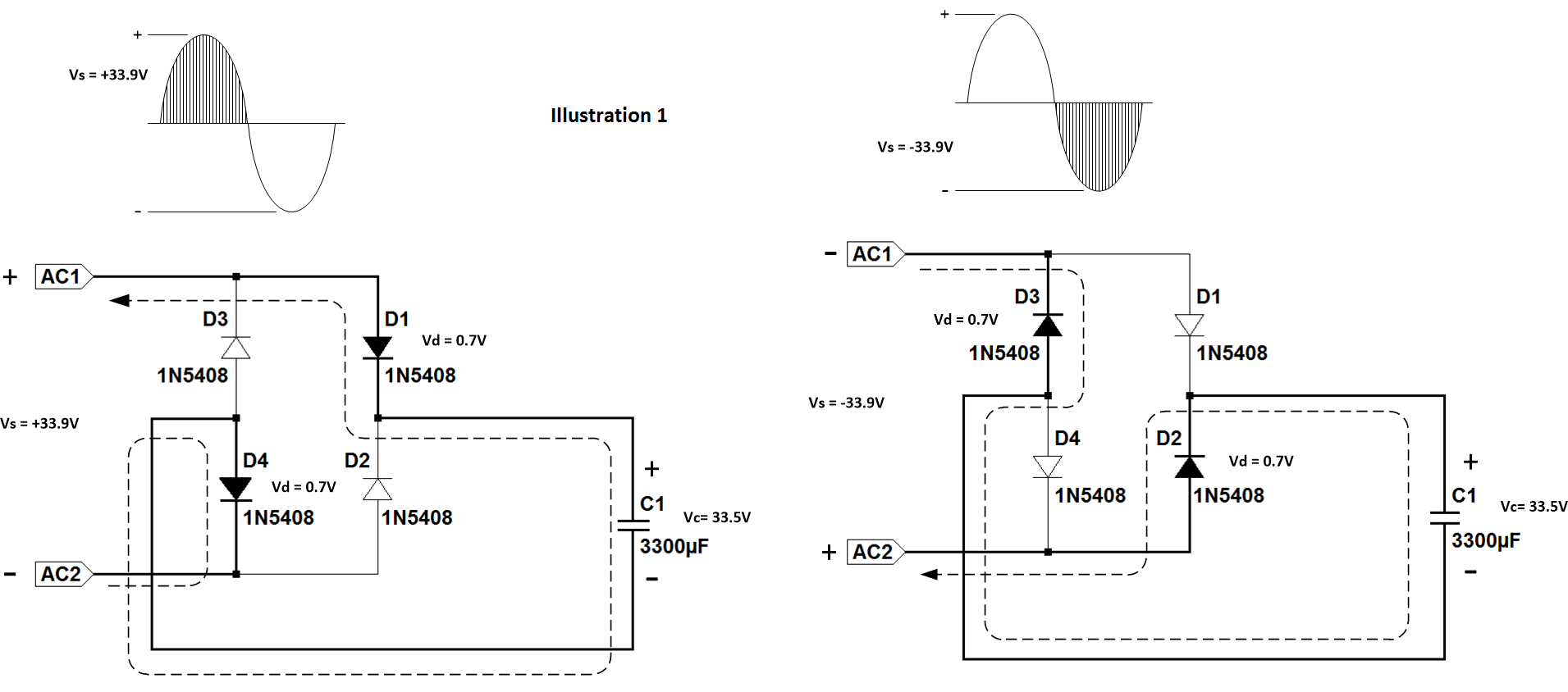
The remainder of the circuit is a -5V power supply for use by the Current Limit, Error Amplifier, and Current Pass function blocks. During the negative half of the AC cycle, C2 is charged through R2 and D3/D5. The time constant of R2/C2 allows C2 to reach an average charge of about +21.5V. R2 also serves to limit the ripple current in C2 to around 60mA which is important as the manufacturers datasheet recommends no more than about 112mA ripple current or reliability will be affected. During the positive half of the AC cycle, C2 discharges into C3 via R2 and D1/D6 until C3 reaches an average charge around -10V. Zener diode D7 then regulates the voltage from C3 down to -5.6V which is then sent to other power supply function blocks. For this supply to work correctly, the transformer must have a secondary voltage of at least 18V RMS. See Illustration 2 below.
Description: The Fan Supply
The fan included with the WeiKedz power supply is a standard DC brushless fan requiring 24V at 100mA. A three-terminal regulator IC U4 (7824) is used to provide a constant 24V output to the fan. Power dissipation for U4 is almost 1W so this part will get very warm during operation. There is no heat sink provided for this part so some convection or forced air flow will be required to keep it from going into thermal shutdown.
Function Block Analysis
Let's take a close look at the components involved and examine a few formula that describe the operation of this portion of the circuit:
A. Surge Current
When the power supply is first turned on, the bridge circuit will see a very large current spike during the first half AC cycle. This "surge current" is the result of charging capacitor C1 from it's initial voltage at or near 0. The magnitude of the surge current depends on the series DC resistance of the transformer secondary winding, the effective series resistance of capacitor C1, the initial voltage of capacitor C1, and the transformer voltage at the time the power supply was turned on. Non-repetitive surge current will not produce enough heat to damage the transformer or C1, but excessive surge current can instantly destroy rectifiers D1 through D4. According to the 1N5408 datasheet, the maximum surge current for one half cycle is 200A. During testing with a suitably sized transformer (Hammond 185G24), the power supply I built produced a surge current of around 40A which is well within the margin of safety.
RESULT: Surge Current performance is ACCEPTABLE
B. V+ and V- Supplies
With no load attached to the power supply, capacitor C1 will charge very quickly to the peak voltage described by the formula below:
V+ = (Transformer Vrms * 1.414) - 1.4
V- = -5.6V (For transformer secondary >= 18V RMS)
So if you do what WeiKedz recommends and attach a 24V RMS transformer to the power supply, both power supplies will reach the following voltages:
V+ = (24 * 1.414) - 1.4 = 32.5V
V- = -5.6V
The total range for both supplies is 38.1V. This is the first problem with the design specifications. There are two integrated circuits, U2 and U3 (TL081), that are connected to both supplies. However the manufacturers datasheet for the TL081 specifies the absolute maximum supply range to be 36V. The recommended supply range for the TL081 is 30V. The manufacturer specifically states that operation outside of the recommended voltage range is not guaranteed and reliability is compromised when absolute maximum ratings are exceeded. For this reason, I do not recommend using a 24V RMS transformer for the WeiKedz power supply.
RESULT: V+ and V- Supply performance is NOT ACCEPTABLE
C. Ripple Voltage and Ripple Current
The peak to peak ripple voltage occurring across capacitor C1 when loaded is approximated by the following formula:
Vripple = I / (2 * f * C) where I is the load current, f is the mains frequency, and C is the value of C1 in Farads.
Ripple is important because it causes heating within the capacitor. The lifespan of a large electrolytic capacitor can be drastically shortened by internal heating due to electrolyte evaporation, can swelling, seal failure, and in extreme conditions explosive failure of the capacitor. For the WeiKedz power supply, the ripple voltage across C1 when the power supply is delivering 3A output current is:
Vripple = 3 / (2 * 60 * .0033) = 7.57V peak to peak
The equation result is an approximation due to the complexity of the actual charge and discharge waveforms on C1. In the power supply I built, the measured ripple voltage was approximately 6V peak to peak while operating at 3A output current.
Due to the many different sizes and voltage ratings of capacitors, manufacturers specify the maximum ripple rating as ripple current in mA. The formulas for determining ripple current in C1 is:
Iripple peak-to-peak = Vripple / sqrt(Xc^2 + ESR^2)
Iripple RMS = Iripple peak-to-peak / (2 * sqrt(3))
Xc = 1 / (4 * pi * f * C) where f is the mains frequency in Hertz and C is the value of C1 in Farads
ESR = DF * Xc where DF is the Dissipation Factor specified by the manufacturer and Xc is reactance of C1
The manufacturers datasheet for C1 indicates that DF is 0.12 and the maximum ripple current is 1.5A RMS. Solving each equation reveals:
Xc = 1 / (4 * pi * 60 * .0033) = 0.402 Ohms
ESR = 0.12 * 0.402 = 0.048 Ohms
Iripple = 7.57 / sqrt(.402^2 + 0.0408^2) = 18.74A peak to peak
Converting the Iripple value from peak-to-peak to RMS results in:
Iripple RMS = 18.74 / (2*sqrt(3)) = 5.4A which is far greater than the manufacturers specifications of 1.5A.
The above calculations show that regardless of output voltage, the power supply cannot deliver 3A without rapid heating and eventual destruction of C1. My actual measurements for ripple current in C1 were almost 4A and the temperature of C1 exceeded 60DegC in a matter of minutes. The best I could achieve without excessive C1 heating was 1A. This is the second problem with the power supply design specifications.
In addition, the ripple voltage on C1 at 3A output current results in the input voltage to the Current Pass function block (Vin) dropping below the 30V output specification (Vout):
Vin = (V+) - Vripple = 32.5V - 7.57V = 24.94V
Since Vin to the Current Pass function block must be greater than or equal to (Vout + 1.4), it is not possible for the power supply to produce a 30V DC output voltage (Vout) when the load current is 3A. The best I could achieve was a DC voltage of about 26V superimposed with a 6Vpp 120 Hz ripple voltage. Not good. This is the third problem with the power supply design specifications.
RESULT: Ripple Voltage and Current NOT ACCEPTABLE
D. Bridge Rectifier Peak Inverse Voltage and Average Forward Current
The two most important parameters for the rectifiers in the bridge section is Peak Inverse Voltage (PIV) and Average Forward Current (IFavg). PIV is the maximum voltage that can be placed across a rectifier in the non-conducting direction. Exceeding this specification can cause the diode to short circuit and burn out, a condition called avalanche breakdown. IFavg is the maximum average current that the rectifier can carry in the conducting direction. Exceeding this specification can cause the diode to overheat and burn out, a condition called junction thermal breakdown.
In a full-wave bridge rectifier, the maximum reverse voltage is equivalent to the transformer secondary peak voltage less one diode voltage drop. The formula for this is:
PIV = ( Transformer Vrms * 1.414 ) - 0.7
If you accept the WeiKedz specification and attach a 24V RMS transformer to the power supply the bridge rectifier PIV voltage will be:
PIV = ( 24 * 1.414 ) - 0.7 = 33.24V
The datasheet for the 1N5408 rectifier indicated that PIV should be no more than 1000V so there is no problem here.
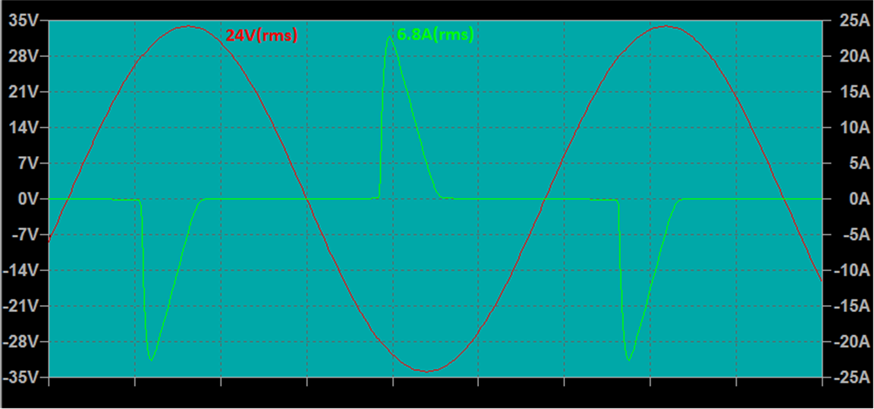
The datasheet specifies that the maximum average forward current can be no more than 3A. In a bridge rectifier configuration, each diode conducts 1/2 of the average current drawn by the load and filter capacitors. In a well designed full-wave bridge circuit, the rectifier current when conducting will be a very large but very short pulse (See Illustration 3). This pulse represents the energy needed to charge the filter capacitor back to peak voltage while powering the load at the same time. Because the pulse usually lasts less than 2ms of a 16ms rectifier conduction cycle, the rectifier current averaged over the entire 16ms cycle will be much lower than the peak current. In the WeiKedz power supply, the Average and Peak current while the bridge rectifiers are conducting is approximated by the following equations:
Iavg = I * ( 1 + pi * ( sqrt ( 2 * Vp / ( Vp - Vr )))) Where I is the Load Current in Amps, Vp is C1 peak voltage, and Vr is C1 ripple voltage.
Ipeak = I * ( 1 + 2 * pi * ( sqrt ( 2 * Vp / ( Vp - Vr )))) Where I is the Load Current in Amps, Vp is C1 peak voltage, and Vr is C1 ripple voltage.
Rectifier conduction time is approximated by the equation:
Dct = [ sqrt ( 2 * ( Vp - Vr ) / Vp ) ] / ( 2 * pi * 120 ) Where Vp is C1 peak voltage and Vr is C1 ripple voltage.
And the Rectifier Average Forward Current for an entire cycle is:
IFavg = Iavg * Dct * 60
Solving these equations for the maximum specified output current of 3A then gives a good estimate of the expected IFavg for rectifiers D1 through D4:
Iavg = 3 * ( 1 + pi * (sqrt ( 2 * 32.5 / ( 32.5 - 7.57 )))) = 18.22A
Ipeak = 3 * (1 + 2 * pi * (sqrt ( 2 * 32.5 / ( 32.5 - 7.57 )))) = 32.44A
Dct = [ sqrt ( 2 * ( 32.5 - 7.57) / 32.5) ] / ( 2 * pi * 60) = .0016 seconds
IFavg = 18.22A * .0016 * 60 = 1.75A
According to the 1N5408 datasheet this current is good for an ambient temperature up to about 90 DegC (194 DegF) which is more than sufficient for most lab situations.
RESULT: Rectifier Reverse Voltage and Forward Current ACCEPTABLE
E. Transformer Selection
WeiKedz isn't very clear on transformer selection and that appears to be one of the largest complaints with the product. So I thought I would address a simple method here. In their defense, WeiKedz recommends an 80W or greater 24V RMS transformer. But which manufacturer and part number? Manufacturers specify transformers in VA (Secondary Voltage and Current) not Watts so what should the current be?
I use a simple equation and a parts list from Hammond Manufacturing or Triad Magnetics to choose a transformer. A bridge rectifier with capacitor filter is known to have a very poor power factor of between 40% and 55% due to the large peak current, narrow conduction angle of the rectifiers in the bridge, and reactance of the filter capacitors. In the power supplies I've designed, the power factor from no load to full load averages 50%. This makes the following equation a good choice for transformer sizing and one I've used successfully for general purpose power supplies:
Transformer VA Rating = (( Vp - ( Vr / 2 )) * Io ) / PF
Where Vp is the peak voltage of C1 for a given transformer secondary RMS voltage, Vr is the ripple voltage on C1 for a given power supply output current, Io is the power supply output current, and PF is the power factor. Check the sections above for how Vp and Vr were determined.
Solving for the Weikedz power supply with a 3A output current gives:
Transformer VA Rating = (( 32.5 - ( 7.57 / 2 )) * 3 ) / .55 = 156.63
To determine the transformer secondary current divide the Transformer VA Rating by the transformer secondary RMS voltage:
Transformer Secondary Current = Transformer VA Rating / Transformer Secondary Voltage =
156.63 / 24 = 6.53A
Below is the oscilloscope trace for the kit I built with a brief 3A load.
Looking through the Hammond Manufacturing catalog, the 185G24 with a secondary of 24VAC and 7A would work perfectly if it weren't for the problems listed above that will prevent the power supply from operating reliably long term.
Looking through the Triad Magnetics catalog, the VPS24-7300 with a secondary of 24VAC and 7.3A would work perfectly if it weren't for the problems listed above that will prevent the power supply from operating reliably long term.
Both of the transformers are available from Mouser and Digikey for around $35.00
The datasheets for the major components in this function block are included below:
1N5408 Rectifier Datasheet is >>> HERE <<<
1N752 Zener Diode Datasheet is >>> HERE <<<
1N4148 Diode Datasheet is >>> HERE <<<
L7824 Regulator Datasheet is >>> HERE <<<
Electrolytic Capacitor Datasheet is >>> HERE <<<
2. Analysis - Reference Circuit
Well. For a seemingly simple circuit, the last section was quite complicated to explain. Fortunately the next few sections are quite a bit easier to describe and understand.
As mentioned earlier the Reference Circuit is the heart of the power supply because it provides the measurement standard that controls both output voltage and output current. This circuit may look complicated because it uses an OpAmp IC, but as you'll see it's actually very simple.
A brief description of an Operational Amplifier
The TL081 (datasheet attached below) is a single OpAmp in an 8-pin DIP optimized for precision low-power applications. It comes close but is not quite equal to the ideal characteristics of an OpAmp:
A. Infinite input impedance
B. Infinite open-loop voltage gain
C. Infinite common mode rejection
D. Infinite signal bandwidth
E. Zero output offset voltage
F. Zero output impedance
G. Zero sensitivity to variations in power supply voltage (V+, V-)
The TL081 OpAmp has two inputs A (non-inverting) and B (inverting), and one output. The equation that defines the output voltage with respect to the input voltages A and B is simply:
Vo = A * (Va - Vb) where A is the open loop gain, Va is the voltage in the "+" (non-inverting) input terminal and Vb is the voltage on the "-" (inverting) input terminal.
If the OpAmp open loop gain is infinite, common mode rejection is infinite, and output offset voltage is zero, then:
Vo = 0, when (Va - Vb) = 0
Vo = V+ (V+ is the positive power supply voltage), when (Va - Vb) > 0
Vo = V- (V- is the negative power supply voltage), when (Va - Vb) < 0
This property is very useful in control circuits like those used in the WeiKedz variable power supply and we'll be using it to describe how the Reference, Error Amplifier, and Current Limit functions work.
The OpAmp is capable of doing far more than this, but I recommend you purchase a good book on Operation Amplifiers if you would like to learn more.
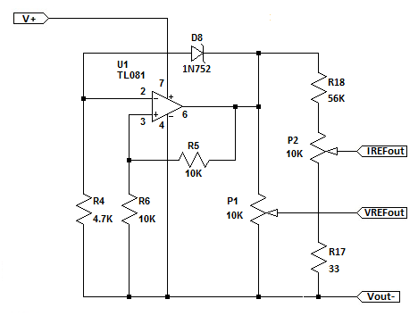
Reference Circuit Operation
Observe the Reference Circuit schematic and you'll notice that the voltages on the A and B inputs of the TL081 are easy to describe:
Va = Vo * R6 / ( R5 + R6 )
Vb = Vo - Vz where Vz is the zener diode voltage
The output voltage Vo depends on Va and Vb according to the equation:
Vo = A * (Va - Vb)
If A is very large, then Va and Vb will need to be almost exactly the same for Vo to settle at some value other than +V and -V. What we need to know is the value of Vo after the circuit powers up and Va and Vb stabilize. An easy way to do this is write the OpAmp equation expanding Va and Vb, set Vo on the left side of the equation to 0, and then solve for Vo on the right side of the equation:
Vo = A * (Va - Vb)
then
0 = A * [ ( Vo * R6 / ( R5 + R6 ) - ( Vo - Vz ) ]
Next plug in the known values for R5 (10K), R6 (10K), and Vz (5.6). For now, assume we don't know what A is:
0 = A * [ ( Vo * 10K / ( 10K + 10K ) - ( Vo - 5.6 ) ]
0 = A * ( Vo * 0.5 - Vo + 5.6 )
Last, rearrange the equation to solve for Vo:
0 = ( A * Vo * 0.5 ) - ( A * Vo ) + ( A * 5.6 )
- ( A * 5.6 ) = ( A * Vo * 0.5 ) - ( A * Vo )
- ( A * 5.6 ) = A * Vo * ( 0.5 - 1 )
- ( A * 5.6 ) / A = Vo * ( 0.5 - 1 )
- ( 5.6 ) = Vo * ( 0.5 - 1 ) notice that A ended up getting cancelled out so we didn't need to know its value
Vo = -5.6 / -0.5
Vo = 11.2V notice that the signs cancelled leaving a positive result
So for a Zener voltage of 5.6V, the OpAmp multiplies that voltage by 2 and produces an +11.2V reference voltage for Vo.
The reference voltage is then sent to the Voltage and Current potentiometers (P1, P2) that allow selection of the power supply output voltage and output current.
Questions and Answers
1. Why use an OpAmp?
The primary advantage of this circuit is that the reference output voltage Vo is virtually unaffected by the ripple voltage on C1. The output Vo of a good OpAmp is insensitive to changes in V+ or V- as long as Vo is kept somewhere in between. A Zener diode by itself, due to it's internal impedance, would be sensitive to ripple voltage on C1 which would result in a significant amount of ripple voltage on the power supply output.
2. Why use a 5.6V Zener Diode?
You'll notice on the circuit board that the zener diodes are marked as 5V1 (5.1V) but the parts supplied are actually 5V6 (5.6V). The reason the 5.1/5.6 diodes are used is due to their lower temperature coefficient which helps the power supply maintain a stable output voltage over a wide temperature range. One manufacturer may offer a better temperature coefficient on their 5.1V part while another offers the same on their 5.6V part. So I suspect (or I hope) that WeiKedz chose a part that offered better temperature stability. Attached in the PDF below are a few examples of the temperature coefficient seen from typical zener diodes.
3. Why use a reference voltage of 11.2V?
I'm now guessing as to what was on the mind of the person that designed the power supply, but based on my testing I believe the WeiKedz power supply was intended to provide 0-20V, not 0-30V as claimed. A 5.1V zener will provide a 10.2V reference while a 5.6V zener will provide a 11.2V reference. Both of these are reasonably close to 1/2 of the power supply output voltage range which helps prevent ripple voltage on C1 from affecting the reference output voltage.
4. Can I hack it?
Yes you can. Now that you know how the circuit works and what it is good for, you can use it in your own projects. To change the output voltage, simply determine the voltage you want and divide by 2, then select a zener diode with the closest voltage:
Vzener = Vo / 2
The "divide by 2" part is determined by the ratio of R5 and R6. So you can also change the output voltage by leaving the zener voltage where it is but changing R5 and R6 using the following formula:
Reference Multiplier = 1 + ( R6 / R5 )
Below are a few resistor values for different multipliers:
Multiplier x2, R5 = 10K, R6 = 10K
Multiplier x3, R5 = 10K, R6 = 20K
Multiplier x4, R5 = 10K, R6 = 30K
A precision 50K 10-Turn trimmer resistor could be used for R6 allowing the multiplier to be continuously adjusted up or down as needed instead of changing the zener diode.
Don't change the Reference voltage on the WeiKedz power supply without reading about the Error Amplifier and Current Limiter as both are designed to work with 11.2V. After you understand both of these functions, you can make the changes you want and the power supply will work as you intended.
Datasheets:
TL081 Operational Amplifier Datasheet is >>> HERE <<<
1N752 Zener Diode Datasheet is >>> HERE <<<
Temperature Coefficient Chart for Zener Diodes is >>> HERE <<<
3. Analysis - Error Amplifier Circuit
The Error Amplifier measures the power supply output voltage, compares it to the set-point voltage selected by the user, and tells the Current Pass function to raise or lower the output voltage until it matches the set-point voltage. How this is done is actually very simple but first let's take a look at a few ancillary portions of the schematic:
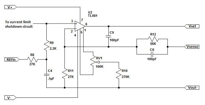
Reference Input Low Pass Filter
Notice that the set-point voltage from potentiometer P1 in the Reference Circuit passes through R8, R9, and C4 before it gets to the non-inverting input of U2. These components serve two functions:
A. Low pass filter for P1/P2
R8 and C4 form a low pass filter with cutoff frequency of:
Fc = 1 / ( 2 * pi * R * C )
Fc = 1 / ( 2 * pi * 27000 * .0000001 ) = 59 Hz
This prevents AC and RF noise pickup on the potentiometer wiring from affecting the power supply output.
B. Regulator Soft Start
To avoid power supply output ringing and possible oscillation during startup and after a current limit event, the time constant of R8 and C4 smoothly raises the output voltage over a time period of 14ms as defined by the following equation (See Illustration 1):
t = 5 * R * C
t = 5 * 27000 * .0000001 = .014 seconds
Error Amplifier Offset Null
Operational Amplifiers aren't perfect and sometimes the IC output doesn't reach the exact voltage expected due to IC variation, temperature, and external component tolerances. The difference between the expected output voltage and the actual output voltage is called the "offset voltage". Normally this voltage is very small and doesn't affect the operation of a typical OpAmp circuit. But in precision control circuits it can be critical that offset be removed or "nulled out". The TL081 provides an optional set of pins to do this. Trimmer resistor RV1 and fixed resistor R10 comprise the external null adjustment for IC U2.
The TL081 datasheet and the TI best practices (attached below) recommend using a 100K trimmer resistor attached to the offset null and Vcc- pins. For the TL081, an additional 1.5K resistor is used to avoid shorting either offset null pin to Vcc- when the trimmer resistor is rotated to the left or right extreme. What this arrangement does is balance the current mirror output in the differential amplifier section of the OpAmp IC (See section 8.2 of the TL081 datasheet).
However, the WeiKedz design does not attach the trimmer resistor to Vcc- and the tail resistor R10 is 270K instead of the recommended 1.5K. The value of R10 (270K) was likely chosen so that the offset adjustment makes full use of RV1s adjustment range. But the attachment to the power supply output ground is a mystery and may be a design error. This arrangement likely works because the Vcc- voltage is so small (-5.6V) compared to the Vcc+ voltage (+32.5V).
Current Limit Signal
The Error Amplifier input is connected to the Current Limiter output through diode D9. In the WeiKedz power supply I built, this not a over-current shutdown feature. It's actually a fold-back current limit feature that reduces the set-point voltage at the Error Amplifier until the output current falls below the current limit set-point. To completely turn off the power supply voltage output, the current limiter output must be able to go negative by at least -0.7 volts due to the voltage drop on diode D9. This is one reason the negative 5.6V power supply is needed.
And now... The Error Amplifier
I've saved the simplest (maybe) part for last. The Error Amplifier is a simple non-inverting amplifier described by the following standard equation:
Vout = Vref * ( 1 + R12 / R11 )
However, the feedback loop is not connected to the output of U4. It's connected after the Current Pass function which has a DC voltage drop of 1.4V. So the standard equation needs to be modified:
Vout = Vref * ( 1 + R12 / R11 ) + 1.4
The closed-loop DC gain of the amplifier is:
Acl = 1 + R12 / R11 = 1 + 56K / 27K = 3
The Voltage Reference circuit described in the previous step includes a set-point potentiometer P1 which provides a voltage to the Error Amplifier between 0 and 11.2V. The Error Amplifier output to the Current Pass section is therefore between:
Vout = ( Vref * Acl ) + 1.4 = ( 0 * 3 ) + 1.4 = 0V
and
Vout = ( Vref * Acl ) + 1.4= ( 11.2 * 3 ) + 1.4 = 35V
For a given reference voltage range, the Error Amplifier voltage range can be changed simply by changing the values of R11 and R12.
When the set-point reference voltage is set with P1, the error amplifier will continuously compare the power supply voltage to the set-point and and adjust its output voltage up or down so that the power supply output voltage does not change regardless of load current.
However, there are three problems with the Error Amplifier output voltage range:
A. U2 (TL081) Maximum Output Voltage Swing
The datasheet for the TL081 OpAmp specifies that the output can swing no closer than 1.5V of Vcc+ or Vcc-. The maximum output voltage on U2 when the power supply is unloaded is:
Vout = Vp - 1.5 = 32.5V - 1.5V = 31V
Remember that the Error Amplifier is connected to the Current Pass function which drops 1.4V from the Error Amplifier output. So the actual maximum voltage to a test circuit attached to the power supply is:
PSout = Vout - 1.4V = 31V - 1.4V = 29.6V
Keep in mind also that the maximum voltage swing used above is a typical value at 25 DegC. Results will vary. The minimum peak output voltage swing in the data sheet is 3V below Vcc+ which would make the power supply output voltage closer to 28V. There is not enough headroom on U2 to reliably generate a 30V output. This is not a 0-30V power supply.
B. Unregulated output when P1 is rotated to its fullest extent
If you remember from the Rectifier and Filter circuit described earlier, the peak unloaded voltage on C1 was around +32.5V and the power supply schematic shows that C1 is used for the +Vcc supply on Error Amplifier U2. Adjusting Reference potentiometer P1 to its highest range will saturate the output of U2 at 31V resulting in an unregulated 29.6V output from the power supply. The cooling fan included with the kit consumes around 100ma which will produce approximately 1Vpp of ripple out of the supply. This ripple voltage will appear at the power supply output to your circuit, which is highly undesirable.
C. Loss of regulation under load
This problem was also discussed in the Rectifier and Filter circuit. With a 1A to 3A load, the ripple voltage on C1 varies between approximately 2.5Vpp to 7.5Vpp. The power supply I built varied between 2Vpp and 6Vpp. For the Error Amplifier to stay in regulation, its output must be below the ripple voltage on C1:
Vout = Vp - Vr - 1.5V where Vp is the peak voltage in C1 and Vr is the ripple voltage on C1. The 1.5V term is the U2 saturation voltage.
Solving this equations for a variety of output currents reveals:
Vp = 32.5V, Vr = 2.5V @ 1A
Vout = 32.5V - 2.5V - 1.5V - 1.4V = 27.1V
PSout = 27.1V - 1.4V = 25.7V
Vp = 32.5V, Vr = 5V @ 2A
Vout = 32.5V - 5V - 1.5V = 26V
PSout = 26V - 1.4V = 24.6V
Vp = 32.5V, Vr = 7.5V @ 3A
Vout = 32.5V - 7.5V - 1.5V = 23.5V
PSout = 23.5V - 1.4V = 22.1V
So the maximum regulated power supply output voltage is between 22.1V and 25.7V depending on load current.
A 5.6K fixed resistor or 10K trimmer inserted above potentiometer P1 will allow the voltage set-point range to be reduced so that regulation will be maintained throughout the full rotation of P1 for all load currents. But this solution limits the power supply output voltage range to 0 - 20V. And it doesn't address the other problems discussed earlier.
Error Amplifier Feedback Frequency Response and Slew Rate Limiting
The Error Amplifier is as its name suggests, is an amplifier. It has gain. As such, if careful design steps aren't taken an amplifier can reinforce noise and harmonic frequencies generated by your test circuit or become a high frequency oscillator just sitting on the bench, which will do your test circuit and your lab not a bit of good. To prevent that, two features were added to the Error Amplifier circuit:
Feedback Low Pass Filter
The addition of C6 to feedback resistors R11 and R12 form a low pass filter with cutoff frequency approximately 32Khz.
Slew Rate Limiter
The TL081 OpAmp has a maximum slew rate of 13V/uS (13,000,000V/S !!!) which is exceptionally fast for such a simple low-cost IC. It is capable of moving from the recommended +V power rail to the -V power rail in about 2uS. The addition of C9 between the U2 output and inverting input pin limit the OpAmp slew rate to around 50uS. Without C9 the output of U2 tends to overshoot and ring with sudden changes in the power supply output voltage. C9 also ends up in parallel with C6 to drop the feedback filter cutoff frequency to 16Khz. Frequency response rolls of to unity gain around 100Khz which helps prevent the power supply from becoming an oscillator.
Datasheets:
TL081 Operational Amplifier Datasheet is >>> HERE <<<
TI Offset Null Recommendations is >>> HERE <<<
4. Analysis - Current Limit Circuit
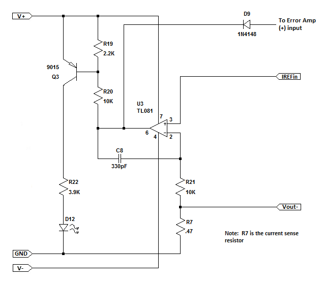
The current limiter circuit is one of the simpler function blocks. It's job is to measure the voltage on the current sense resistor and compare it to the current set-point voltage. Initially the output of the limiter is near the V+ power rail, but switches toward the V- power rail when the current set-point is exceeded. This reduces the reference voltage to the Error Amplifier and keeps the regulator output current at the current set-point.
Voltage Comparator
Remember how an ideal OpAmp works and this circuit is easy to understand. The equation for the output of U3 is:
Vo = A * (Va - Vb) where Va is the voltage on the non-inverting (+) input pin and Vb is the voltage on the inverting (-) input pin.
When there is no feedback network attached to U3, gain A is a very large number so the output of U3 can be described as follows:
Vo = 0, when (Va - Vb) = 0
Vo = V+ (V+ is the positive power supply voltage), when (Va - Vb) > 0
Vo = V- (V- is the negative power supply voltage), when (Va - Vb) < 0
This is the simple definition of a voltage comparator. In practical circuits, however, it is nearly impossible for Va and Vb to be equal so the last two equations are the ones that are important.
Current Sensing
The current sense resistor R7 is a small value power resistor (sometimes referred to as a "shunt") that works as a current-to-voltage transducer. It's value must be small so that only a minimal amount of energy is lost, but it also must be large enough to produce a measurable voltage for U3. The relationship between the current through R7 and the voltage on R7 is:
Vr = I * R where I is the power supply output current and R is the value of R7. So for various output currents the voltage on R7 is:
Vr = 0 * 0.47 = 0V when I is 0 Amps.
Vr = 1 * 0.47 = 0.47V when I is 1 Amp.
Vr = 2 * 0.47 = 0.94V when I is 2 Amps.
Vr = 3 * 0.47 = 1.41V when I is 3 Amps.
The current sense voltage can vary between 0V and 1.41V when output current varies between 0A and 3A. This is the voltage range that will be compared to the current limit set-point voltage.
You will notice that R7 is physically large. Even though the resistance of R7 is small, the current through it will be quite high and a good deal of heat will be produced. The surface area of R7 needs to be large enough for that heat to be exchanged with the surrounding air. Otherwise R7 can become so hot it self destructs. The work done (Power) in the form of heat in Watts by R7 is described as:
P = Io^2 * R7 where Io is the power supply output current
Solving this equation for the power supply maximum rated current of 3A results in:
P = 3^2 * 0.47 = 4.23W
This is dangerously close to the 5W maximum rating of R7. At 4.3 W power the resistor surface temperature will reach 117 Deg C (242 Deg F) in less than a minute. "Don't touch this" comes to mind and that heat needs to be removed if the power supply is placed in an enclosure. The WeiKedz kit provides a fan for this but you will need to remove it from the heatsink so that air can be moved across the entire power supply, not just the heat sink.
Current Limit Set-Point
Potentiometer P2 is used to provide the set-point current limit voltage. It's a simple voltage divider composed of P2, R17, and R18. The set-point voltages that can be obtained from P2 are described by:
Vccw = Vref * ( R17 / ( R17 + P2 + R18 )) where Vref is the reference voltage of 11.2V and Vccw is the voltage on U3 Pin3 when P2 is fully counter-clockwise.
Vcw = Vref * (( R17 + P2 ) / ( R17 + P2 * R18 )) where Vref is the reference voltage of 11.2V and Vcw is the voltage on U3 Pin3 when P2 is fully clockwise.
Solving these equations using the known values gives the following voltages for Vccw and Vcw:
Vccw = 11.2 * ( 33 / ( 33 + 10000 + 56000 )) = 0.0056V
Vcw = 11.2 * (( 33 + 10000 ) / ( 33 + 10000 + 56000 )) = 1.70V
Because OpAmp U3 is acting as a voltage comparator its output will shift from V+ to V- only when the current sense voltage is greater than the current set-point voltage. So the minimum and maximum power supply output currents can be calculated as:
Iccw = Vccw / R7 = 0.0056 / 0.47 = 12mA
Icw = Vcw / R7 = 1.70 / 0.47 = 3.62A
In the kit I built, I didn't want 3A of current so I changed the value of R18 to 200K which changed the output current limit range between 4mA and 1.14A. You can use the above equations to define your own ranges by changing the values of R17 and R18.
Slew Rate Limiting
As was mentioned in the previous step, the TL081 OpAmp has a maximum slew rate of 13V/uS which allows it to traverse the recommended +V/-V power rails in about 2uS. This is fast enough for parasitic inductance and capacitance to induce ringing and oscillation in the power supply. To prevent that, C8 was added to limit the slew rate from 13V/uS to around 0.3V/uS. Fast enough for the current limiter to do it's job, but not so fast that current control is lost.
Current Limit Indicator
The current limiter includes an indicator feature that lights an LED when current limiting is engaged. When U3 output falls to around 28V, PNP transistor Q3 is forward biased through resistors R19 and R20 as described in the formula:
Vo = ( V+ ) - ( VBEsat * ( R19 + R20 )) / R19 where V+ is the voltage on C1 and VBEsat is the forward biased base-emitter saturation voltage for the SS9015 PNP transistor (see data sheet below).
Solving this equation results in:
Vo = 32.5 - ( 0.82 * ( 2200 + 10000 )) / 2200 = 27.95V
When Q3 turns on, almost the full V+ voltage is applied to R22/D12. Typical maximum LED current is 20ma to 30mA with a forward voltage of 2V to 3V so it's best to check the datasheet or test the LED before deciding on the value of R22. The LED I received in the WeiKedz kit turned on at 2V forward voltage with almost 2.4V at 10mA. The designer of the kit elected to limit diode current to approximately 7.8mA which is plenty of brightness:
ILED = ( V+ - VLED ) / R22 = ( 32.5 - 2.2 ) / 3900 = 7.8mA
Power dissipated in R22 is:
P = ILED^2 * R22 = .0078^2 * 3900 = 237mW
That's very close to the 250mW rating of R22 but I'll allow it since the LED will only be turned on when the current limiter is activated. The user will then likely intervene and increase the current setting or turn off the power supply.
Datasheets:
1N4148 Diode Datasheet is >>> HERE <<<
SS9015 Transistor Datasheet is >>> HERE <<<
TL081 Operational Amplifier Datasheet is >>> HERE <<<
5. Analysis - Current Pass Circuit
The Current Pass function is the workhorse of the power supply. It's job is provide a fixed output voltage regardless of the size of the load attached to the power supply (depending on the current limit set-point or the maximum current rating of the supply).
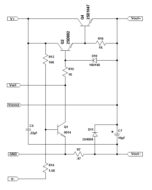
The active elements in this function block are Q2 (2SD882) and Q4 (2SD1047). These two transistors are wired in a Darlington configuration which provides an extremely high input impedance (>50K Ohms) to the Error Amplifier and a very low output impedance (<0.1 Ohms) to the load and very high DC current gain (>10,000). The Darlington configuration comes with a few disadvantages:
A. Output voltage is 1.4V lower than the input voltage due to the combined Base/Emitter junctions of Q2 and Q4.
B. Slower switching speed due to Base-Emitter capacitance of Q4.
C. Higher power dissipation in Q4 when used as a switch due to 0.7V saturation voltage limitation.
There is nothing we can do about the first limitation other than account for it in the design. To minimize the effect of B-E junction capacitance in Q4, it is common to add a resistor (R16) between the Base and Emitter terminals of Q4. This is a recommended practice but not strictly needed in a general purpose analog variable power supply. Testing of the WeiKedz power supply I built shows no change in the performance of the Current Pass function when R16 is omitted. The slew rate limiting applied to the Error Amplifier and Current Limit functions eliminate any benefit of R16. The 3rd limitation doesn't apply to an analog variable power supply.
The output voltage is described by the following equation:
Vout+ = Vset - 1.4
Notice that the Error Amplifier voltage sense input is connected to the output of the Current Pass function, so the 1.4V drop in Q2/Q4 is automatically accounted for. The error amplifier output voltage will always be 1.4V higher than the desired output voltage of the power supply.
All other components in the schematic are ancillary functions. Q2 and Q4 are doing all of the work. There is one issue with the WeiKedz design as you'll see when reviewing the datasheet for Q2 (2SD882):
When the power supply output voltage is set to 0V, the maximum Vceo rating of Q2 is exceeded by 2V (see attached 2SD882 datasheet). The transistor Base terminal is not open-circuit as specified in the rating, but exceeding Vceo under any circumstances is bad practice. Temperatures higher than 25DegC can result in the Collector-Emitter junction breaking down unexpectedly. A C-E short-circuit in Q2 will cause the power supply output to suddenly change to V+ (32.5V) with current limiting disabled, potentially destroying the circuit attached to the power supply. This is further evidence that the WeiKedz power supply was not designed for 0-30V as specified.
-5V Failure Shutdown
The -5V supply is required for the variable power supply to operate properly. Without it, the Error Amplifier and Current Limit functions become unstable. R13, R14, and Q1 form a shutdown circuit for the Current Pass function if the -5V power supply falls below approximately -3.8V. Q1 will be saturated by R13 shorting the output of Error Amplifier U2 to ground, which turns off Q2 and Q4 and drops the power supply output to 0 volts. U2 is internally protected from short circuit to ground or to either of the power supply pins.
However the maximum U2 IC dissipation (650mW at 25DegC) cannot be exceeded during an output short circuit event. This is not a problem when operating the TL081 at the recommended +/- 15V power supply voltages. Short-circuit output current for the TL081 is internally limited at 20mA. But when using a +32.5V supply and adding in the TL081 operating current of 1.4mA, shorting U2 output to ground will result in 700mW of device dissipation. This is a bad thing if the -5V supply fails and the operator doesn't notice. U2 will likely overheat and self destruct. During testing of the power supply I built, lifting R14 from the PCB overheated U2 in less than a minute. Using a 20VAC transformer instead of a 24VAC transformer reduced U2 dissipation to 500mW which is still high but manageable. Yet one more data point that makes me believe this power supply circuit was not intended for a 30V output.
C7 Discharge
C7 is included to improve output voltage stability when powering circuits with small but rapid changes in load current. However, C7 doesn't have a low impedance discharge path if no load (or very light load) is attached to the power supply. The only path available is the large value resistors R11/R12 (83K Total) in the Error Amplifier. If the power supply output voltage is set to maximum, and then quickly set to zero, Q4 Base-Emitter junction will be reverse biased and no current will flow through the Current Pass function. It will then take over 4 seconds for C7 to discharge through R11/R12 according to the following:
Discharge Time = R * C * 5 = ( 56000 + 27000 ) * .00001 * 5 = 4.15 seconds
This will be visible if a volt meter is used to measure the power supply output, and can make adjusting the power supply difficult without a load attached.
To prevent this, D10 and R15 were included to provide a low impedance discharge path for C7. If the reference voltage falls below the output voltage, D10 will be forward biased which results in R15 being connected across C7. The discharge rate for C7 will then be:
Discharge Time = R * C * 5 = 1000 * .00001 * 5 = .05 seconds
R11/R12 were not included in the above equation because their combined value is so large that R15 dominates.
Reverse Output Voltage Protection
To protect the power supply from reverse voltages attached to the output (charged capacitors, batteries, another power supply, etc.) diode D11 is attached across C7. If a voltage greater than -0.7 volts is attached to the power supply output, D11 will conduct preventing the voltage from rising further until the offending voltage is removed or D11 is destroyed.
Datasheets:
1N4004 Rectifier Diode Datasheet is >>> HERE <<<
1N4148 Diode Datasheet is >>> HERE <<<
2SD882 Transistor Datasheet >>> HERE <<<
2SD1047 Transistor Datasheet >>> HERE <<<
SS9014 Transistor Datasheet >>> HERE <<<
6. Assembly Manual for Transformer Operation
I've re-written the assembly manual for the WeiKedz Variable Power Supply to make it easier to follow and included some part placement and soldering tips for those wanting the benefit of better illustrations before attempting an this electronics project.
I've also included an Operation and Maintenance guide for use after the project is assembled. This guide will provide some assistance and suggestions for attaching a transformer to the power supply, and also includes detailed description of each power supply function block.
Assembly Manual is >>> HERE <<<
Component Identifier is >> HERE <<
Operation and Maintenance Manual is >>> HERE <<<
This concludes Part 1 of the Portable Variable Power Supply article which hopefully has given you a solid understanding of how the Weikedz power supply works. Next, I'll describe how to put the information to use modifying the power supply from transformer to battery operation, and how to add a V/I meter to make a more useful portable variable power supply.