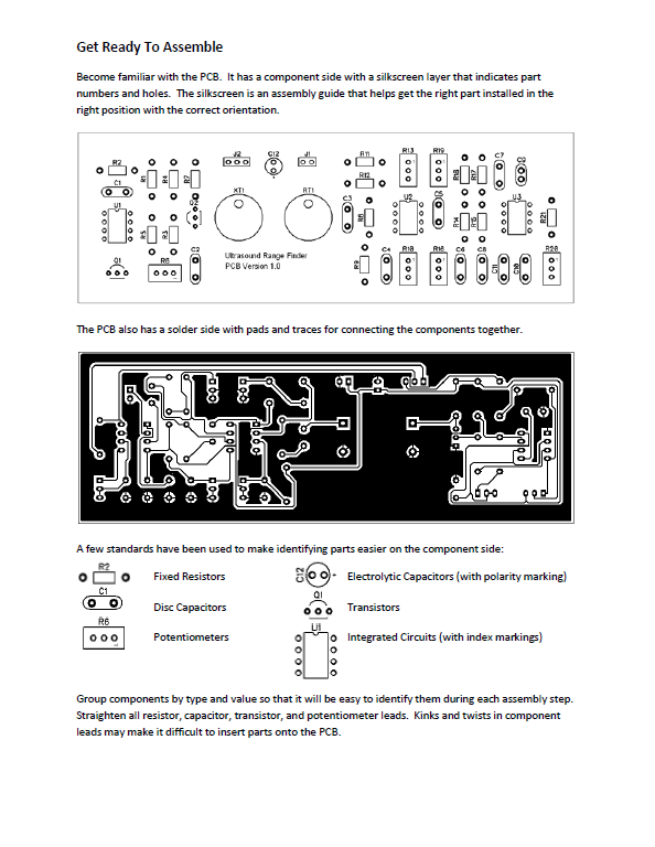
When I started my career in control systems I was fascinated with the many different ways that machines could be interfaced to the environment they operated in. Limit switches (electrical and optical), encoders, resolvers, strain gauges, thermocouples... the control system engineer had a long list of sensors to choose from. And the list has grown even longer following successful innovations in micro machining. Today the sensor and conditioning electronics, and even a microprocessor for signal processing, are integrated on a chip. Sensor integration has helped make machine control systems smaller and easily distributed throughout a given process. But they have also obscured what actually goes on inside the black box. As a design engineer, I enjoyed reading schematics and taking sensors apart to figure out how they did what they did. I learned quite a bit about how noisy and stressful the outside world is on sensitive electronics, and how challenging it can be to reliably separate out a desired signal from industrial background noise.
At first glance, the theory behind an ultrasound range finder seemed intuitive and there were a number of small and inexpensive ultrasound sensors available commercially. But all of these are highly integrated mixed-signal products that would have been difficult to fully understand and experiment with using an oscilloscope and pulse generator. So I decided to design my own and see how ultrasonic waves propagate, reflect, and interfere in a given space. My goal was to design a circuit that could reliably detect an object 1 to 10 feet from the sensor using digital control signals from a small computer like a Raspberry Pi or Arduino. The analog ultrasound range finder would generate the carrier pulse and detect the carrier reflection. The computer would control transmitter timing and convert the carrier reflection time delay into a distance.
This project was a fun exercise in simple analog design with digital interfacing and software programming. For those interested in giving a project like this a try I've included a very detailed assembly manual, lots of pictures, theory of operation, parts list, software, and complete schematics.
Obtain The Assembly Manual
The Analog Ultrasound Range Finder project in this article was constructed by following the steps in the Assembly Manual found >>> HERE <<<. The assembly manual contains the following useful information:
1. Basic soldering and assembly techniques.
2. Step-By-Step illustrated assembly instructions.
3. Testing and Alignment Procedure.
4. Troubleshooting Procedure.
5. Parts List.
6. Circuit Schematics
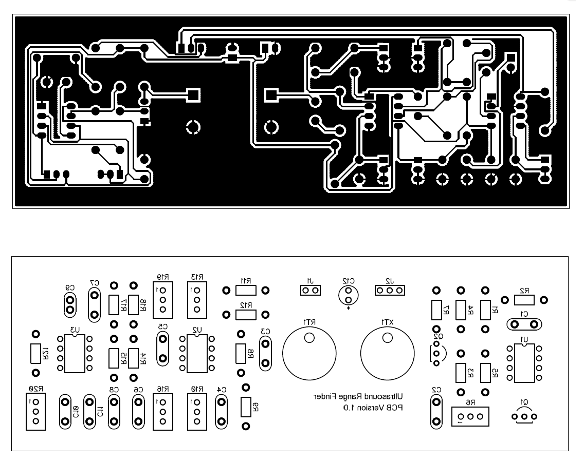
The PCB layout for the range finder project was made using the free version of Diptrace (www.diptrace.com) which works really well for small projects on double-sided or single-sided boards. The Diptrace schematic files, PCB layout files, and PCB toner templates can be obtained at the links below:
For single run prototype PCB projects I use the toner transfer process and materials from Pulsar Professional FX's product "PC Fab-In-A-Box" (www.pcbfx.com). Their process has worked well for me. I run the toner prints with an HP Laserjet P2035 with toner density turned full up. I do the transfers with an Apache AL13P which can do boards up to size A at 390 DegF. After that I sponge on some warmed up Ferric Chloride for a few minutes until unwanted copper is removed. The PCBFX products work really well for the work I do and can reliably lay down some really fine lines.
NOTE: As of 2026, Pulsar Professional is no longer in business. I have left the content here for historical purposes.
Obtain Components Listed in the Assembly Manual Parts List
Review the parts list and obtain the components indicated. Below are a few notes regarding the parts used for the Analog Ultrasound Range Finder:
1. I purchased all of the parts from Mouser (www.mouser.com) but you can obtain them from Digikey, Sparkfun, or another distributor. If you use another source, be sure to review the datasheets to make certain the parts have the same physical dimensions and lead spacing as the ones I've specified or they may not fit on the PCB.
2. 20-Turn trimmer resistors are highly recommended as amplifier and oscillator parameters require fine adjustment.
Please Note: I have no business relationship with any of the above vendors. Nothing of financial value was exchanged for my recommendation. None of the above vendors provided compensation of any kind during the creation of this project. I will not be compensated in any way if you choose to build this project or purchase components from any vendor I recommend. I simply had a good experience with the vendors I recommend and believe you will too.
Review the Schematic to Become Familiar With the Range Finder Transmitter Design
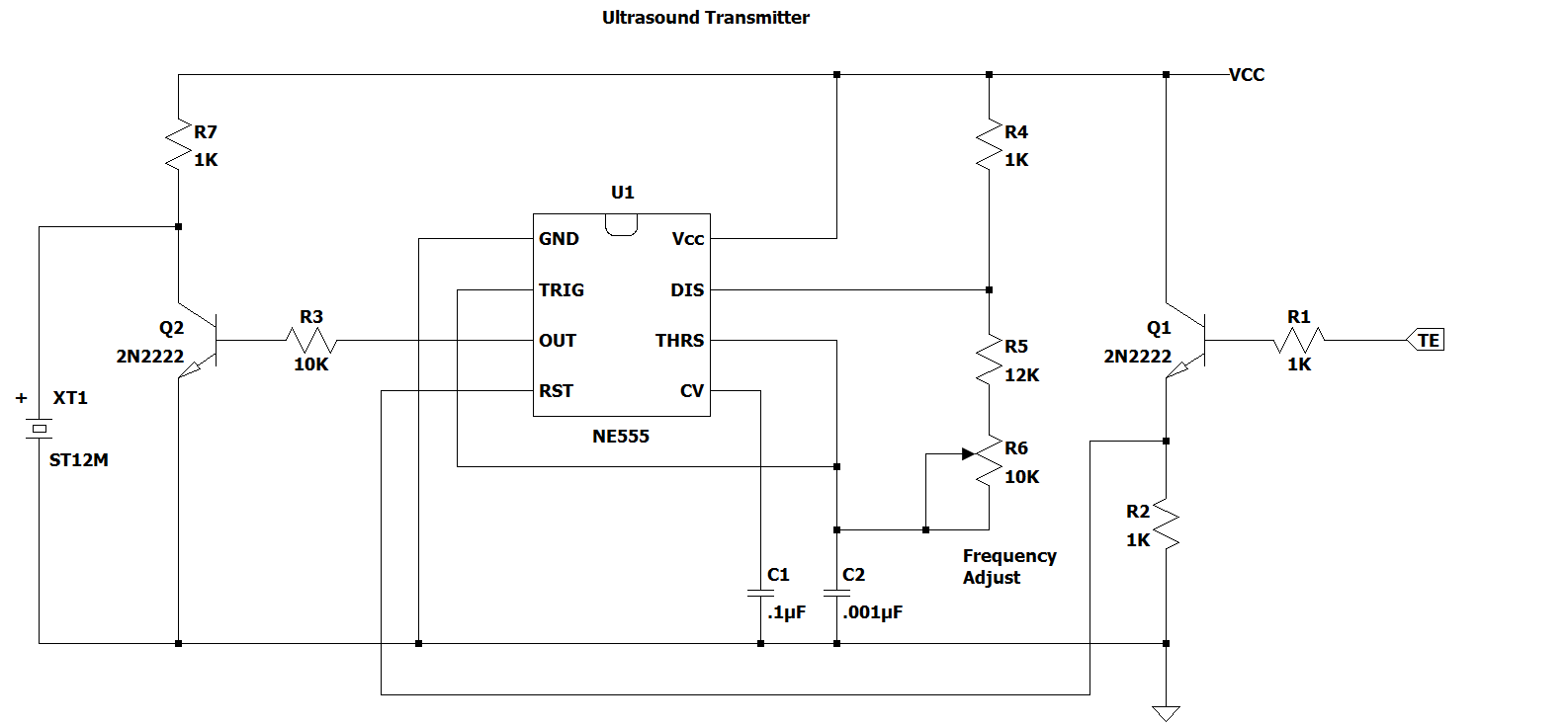
Transmitter Design
The Ultrasound Transmitter is a simple 555 astable oscillator circuit with a frequency of 40KHz and a duty cycle near 50% (i.e. square wave output). I used the circuit topology recommended in the datasheet for an astable oscillator. No sense "reinventing the wheel" when a perfectly good circuit is provided by the manufacturer.
The oscillator is switched on and off via common collector Q1 which is connected to the 555 reset pin. An active high on the base of Q1 brings the 555 timer chip out of reset and oscillation starts. A low voltage on Q1 pulls down the 555 reset pin through R2 and oscillation stops. Q1 isolates control logic from the 555 timer reset current and ensures the reset voltage will fall below the nominal 500mV indicated in the data sheet as the TE pin falls below 1V. The 555 oscillator does not require the Control Voltage pin (Pin 5) so it is bypassed to ground via C1 as recommended in the data sheet.
According to the 555 IC datasheet, two formulas determine the oscillation frequency and the duty cycle of the transmitter output:
Frequency = 1 / (0.693 * (R4 + 2 * (R5 + R6)) * C2)
Duty Cycle = (R5 + R6) / (R4 + 2 * (R5 + R6))
The duty cycle equation indicates that for a near 50% output on/off ratio, the value of of R4 should be very low compared to the combined value of R5 and R6. However, because the Discharge pin will go low to discharge C2 the value of R4 cannot be so low as to cause the 555 IC to exceed its maximum power dissipation. The datasheet provides some guidance on the recommended Discharge pin saturation current (between 4.5mA and 15mA). A discharge saturation current of 5mA was chosen so that a common 1K resistor could be used for R4 (i.e. 5V/5mA = 1K Ohms).
In this circuit configuration the most that the Duty Cycle can practically be is around 49%, so that value is used as a starting point for determining the value of R5 and R6.
Rearranging the Duty Cycle equation to solve for the combination of R5 and R6 results in:
R5 + R6 = R4 / ((1 / DutyCycle) - 2)
Notice in the above equation that the denominator results in a singularity at 50% duty cycle.
Substitute the known values: Duty Cycle = 0.49, R4 = 1000 Ohms
R5 + R6 = 1000 / ((1 / 0.49) - 2) = 24,500 Ohms
Now to check if the above resistance can be used with a standard capacitor value.
Rearranging the Frequency equation to solve for C2 results in:
C2 = 1 / (F * 1.386 * (R5 + R6))
Substitute the known values: F = 40,000 Hz, R5 + R6 = 24,500 Ohms
C2 = 1 / (40000 * 1.386 * 24500) = 736pF
I prefer to use the most common disk capacitor values in order to avoid potentially high costs and supply issues, so for this design I rounded up to .001uF (aka 1000pF).
Now that a suitable value has been chosen for C2, rearranging the Frequency equation to adjust the value of R5 + R6 results in:
R5 + R6 = 1 / (F * 1.386 * C2)
Substitute the known values: F = 40,000 KHz, C2 = .000000001 Farads
R5 + R6 = 1 / (40000 * 1.386 * .000000001) = 18,038 Ohms
I typically try to choose a combination of values for R5 and R6 so that the target frequency is obtained when R6 is adjusted near it's midpoint. This allows plenty of room for adjusting the oscillator frequency up or down as needed. So I chose a 12K Ohm resistor for R5 and a 10K trimmer for R6. By adjusting R6 to around 6K Ohms, the desired 18K Ohms is achieved with plenty of room to adjust for a near exact 40KHz.
Now that suitable values for R5, R6, and C2 have been chosen, the standard Duty Cycle equation can be used to verify the desired duty cycle is near 50%:
Duty Cycle = (12000 Ohms + 6000 Ohms) / (1000 Ohms + 2 * (12000 Ohms + 6000 Ohms)) = 48.6%
Almost perfect! The last step is to add a driver to the 555 IC output.
The 555 IC datasheet indicates that the Output pin (Pin 3) can source and sink 200mA of current, but not at the rated Vcc applied to the chip. In order to obtain the highest voltage swing possible across transmitter XT1, I used a common emitter Q2 in parallel. When the 555 IC output is low, XT1 is driven close to Vcc through R7. When the 555 IC output is high, Q2 shunts XT1 driving it's voltage to near zero. R7 limits the Vcc shunt current through Q2 to 5mA while protecting XT1 from excessive charge current. R3 was chosen to ensure that Q2 fully saturates when the 555 IC Output pin goes high. Transmitter XT1 behaves like a parallel LC resonant circuit tuned to 40KHz with Q of around 40. Therefore, Q2 serves another important purpose: Damping XT1 so that the ultrasound output cuts off within 1ms after the 555 IC is disabled.
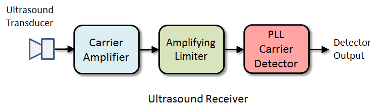
Review the Schematic to Become Familiar With the Range Finder Receiver Design
The receiver design is significantly more complicated than the transmitter design. There are several circuit adjustments provided so that the amplifiers can be reconfigured for different types of receivers (time delay, doppler, interferance, etc). I will cover only the Time Delay receiver type in this article in order to keep it as short as practical.
Simple Sonar Example
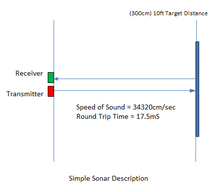
The "Simple Sonar" example above describes what the transmitter and receiver are trying to do. An ultrasound wavefront propagates from the transmitter, bounces off of a target, and is detected by the receiver. By measuring the round trip time between the start of transmission and the detected reflection, and comparing that to the propagation velocity of sound, the distance between transmitter and target can be calculated. The formula is:
Distance = (Round Trip Time / 2 ) * Velocity of Propagation
In the real world, however, the problem is much more complicated as illustrated in the "Complex Sonar" example below. I won't force you through a rigorous explanation of the receiver design math but below are just a few of the parameters that have to be considered:
1. Ultrasound Transmitter Minimum Power and Dispersion Angle
2. Ultrasound Receiver Sensitivity
3. Minimum detector signal threshold
4. Target Reflection Coefficient
5. Distance, Air Density, and Air Flow effects on Sound Attenuation
6. Temperature, Humidity, and Elevation effects on Propagation Velocity
7. Time delay and signal strength effects of multi-path interference
A Real-World Sonar Example
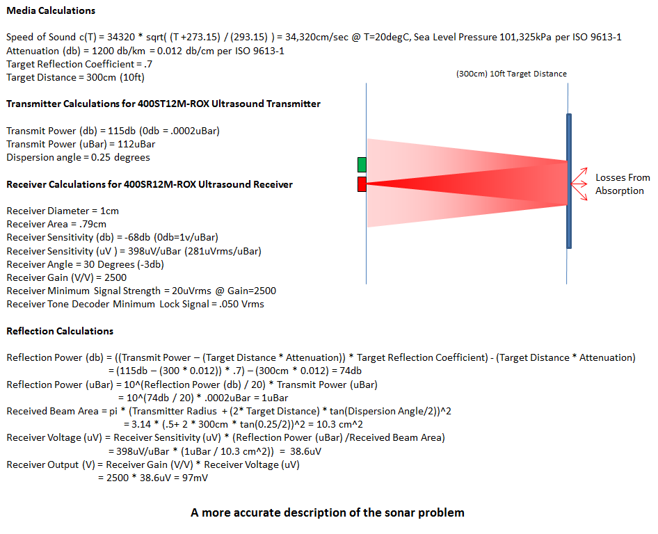
The receiver presented in this article was designed to detect a large, unobstructed, stationary target at a maximum distance of 10 feet, and smaller targets at a maximum distance of 6 feet. The actual distances that can be measured depend on how large the target is, how reflective the target is, how quickly the target is moving, how many obstacles exist between the sensor and the target, and to a lesser extent how active the air is between the sensor and the target.
The ultrasonic transducers used (RT1 and XT1) are piezoelectric devices that are optimized to ether change shape when a voltage is applied (transmitter transducer) or produce a voltage when struck by ultrasonic sound waves (receiver transducer). Both devices use quartz crystals that exhibit reactive properties when energized by an AC signal source. The equivalent circuit for each is a parallel resonant RLC circuit with 2400pF capacitance, 6.6mH inductance, and 1600 Ohms resistance. The receiver transducer has an area of less than 1cm^2 and a sensitivity of 398uV per ubar of sound pressure. We will need an amplifier with input impedance at least 5X the transducer impedance to capture as much of the signal voltage as possible, and the amplifier will need very high gain so that the small transducer voltages can be magnified enough to do something useful.
1. The receiver circuit is intended for a single supply voltage of +5V. So a good Op-Amp for this design is one optimized for a Single Ended Supply (+2.5V to +24V) and Rail-to-Rail Output (+0.1V to +4.99V).
2. The receiver circuit must provide high gain at high signal frequency. So a good Op-Amp for this design needs a high gain bandwidth product, and a high slew rate.
Slew Rate in Volts/uS = 2 * pi * Frequency * Vp * .000001
Gain Bandwidth Product = Frequency * Gain
Substituting the known circuit parameters: Frequency = 40,000 Hz, Vpp = 5V, Max Gain per Stage = 100
Slew Rate = 2 * pi * 40000 * 5 * .000001 = 1.26V/uS
Gain Bandwidth Product = 40000 * 100 = 4,000,000 Hz or 4MHz
3. The amplifiers are standard inverting designs that will operate on a regulated supply, so Power Supply Rejection and Common Mode Rejection aren't critical and can be around 80db which is typical for many Op-Amps.
4. There are two gain stages in this design and the PCB needs to be reasonably small, so a dual Op-Amp in an 8-pin package would be best.
As an analog designer I'm somewhat partial to TI products so entering the target parameters above into their product website shortened the list down to 6 candidates. One Op-Amp stood out as an excellent choice with respect to features and cost:
TI LM6132 Dual Low Power 10 MHz Rail-to-Rail Operational Amplifier
The specifications for this chip exceeded the needed parameters. The trade-off is that the LM6132 can only drive high impedance loads (10K is recommended). But in every other respect, it's a good choice.
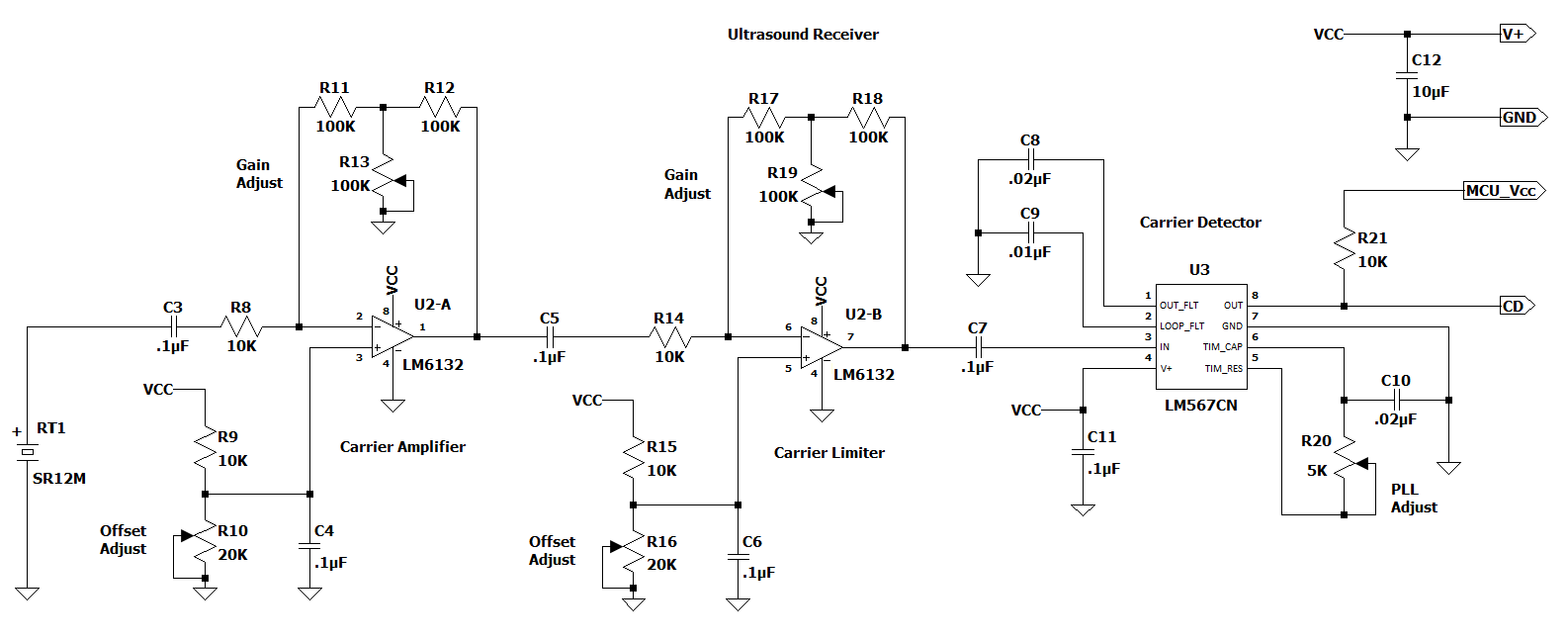
Receiver Design - Carrier Amplifier and Carrier Limiter
The LM6132 is operated with a single +5V power supply, so the amplifier needs an input DC bias voltage to set the output to the desired DC offset voltage. Adjustable voltage dividers R9/R10 and R15/R16 provide the bias voltage to the non-inverting input (pins 3 and 5) of each Op-Amp. Increasing the bias voltage to the non-inverting input increases the output offset voltage. Decreasing the bias voltage to the non-inverting input decreases the output offset voltage. Capacitors C4 and C6 prevent high frequency power supply noise from affecting the Op-Amp output.
The LM6132 data sheet recommends a load resistance of 10K to achieve the output swing and slew rate specifications, so a 10K input impedance was chosen for both amplifiers via R8 and R14. This also meets the design goal of an input impedance roughly 5X the receiver transducer impedance discussed earlier. The standard formula for an Op-Amp inverting amplifier gain (A) is:
A = - Rf / Rin where Rf is the feedback resistor and Rin is the input resistor.
However for a maximum stage gain of 100, the Rf value would need to be 1Meg Ohm. I prefer not to use resistors over 100K in feedback circuits and especially not 1Meg trimmer resistors. They are extremely noisy and difficult to adjust. So instead, for amplifiers with large gains I recommend the modified tee feedback configuration illustrated in the receiver schematic. This feedback circuit is quieter than the simpler 1Meg trimmer design and is easier to adjust. The gain formula using the first stage as the example is:
A = R11/R8 * (2 + R11/R13)
When trimmer resistor R13 is adjusted to 33K Ohms, the Op-Amp gain is set at 50. Resistors R17, R18, and trimmer resistor R19 set the second stage gain the same way.
Receiver Design - Carrier Detector
In order to separate the transmitted carrier signal from external and internal noise, a Phase-Locked-Loop tone decoder IC (TI LM567) is used for the Carrier Detector. The detector output is an active low digital Carrier Detect (CD) signal that is easily interfaced to a micro-controller. The LM567 datasheet indicates that the input impedance in Pin 3 is 40K Ohms, which is more than high enough to keep the LM6132 Limiter output in spec. As recommended in the LM567 datasheet, capacitor C7 decouples the DC output of the Limiter from input Pin 3 and capacitor C11 helps insure a noise free power supply at Pin 4. The PLL oscillator frequency is defined by the following equation:
F = 1 / (1.1 * R * C)
Note: Manufacturers differ on the equation above so be sure to check the datasheet for the part you have!
There are many different values that can be used for R and C. I had a bunch of .02uF disk capacitors in inventory so I decided to use one of them. Rearranging the Frequency equation to solve for R when C is known results in:
R = 1 / (1.1 * F * C)
Substitute the known values: F = 40000 Hz, C = .00000002 F
R = 1 / (1.1 * 40000 * .000000002) = 1136 Ohms
So for the LM567 PLL oscillator, C10 is a .02uF capacitor and R20 is a 5K Ohm trimmer adjusted to 1136 Ohms.
For accuracy at close range, the Carrier Detector needs to lock onto the reflected ultrasound pulse in the fewest number of cycles. The LM567 datasheet indicates that the loop bandwidth and output filter play a role in the responsiveness of the detector output. Referring to the graphs in the datasheet, setting the value for C9 at .01uF allows the LM567 to lock onto the ultrasound pulse within 20 cycles (500uS) but sets the loop filter bandwidth at 14% (which is higher than desired but an acceptable trade). The datasheet recommends that the value of C8 be twice the value of C9 so a value of .02uF was chosen for C8. The LM567 output Pin 8 is an active low open collector transistor that requires an external pull-up resistor. A 10K Ohm pull-up resistor R21 has been included for convenience but the internal pull-up feature on the Raspberry Pi or Arduino I/O can be used instead.
Receiver Design - More about the Carrier Limiter
Notice that the second amplifier stage is referred to as an Amplifying Limiter. This circuit is nearly identical to the Carrier Amplifier with one exception: The input bias voltage is adjusted so that the output offset is 0V when no signal is detected. The reason for this has to do with environmental ultrasonic noise causing false triggering of the Carrier Detector. Many sources of audible noise (snapping your fingers, boiling water, metal shaping, etc.) create weak sound in the ultrasonic spectrum. This noise can cause the LM567 to generate short bursts of activity even when the transmitter isn't turned on. With careful adjustment of the Limiter, background noise can be removed from the Detector input so that the Detector output only triggers when ultrasonic measurements are being made.
Fabricate the PCB for the Range Finder

NOTE: As of 2026, Pulsar Professional is no longer in business. I have left the content here for historical purposes.
I fabricated the PCB for this article using the PCB Fab-In-A-Box starter kit from Pulsar Professional FX at www.pcbfx.com. The company offers a Starter Kit that includes the bare PCB that I used for the Range Finder board, a bunch of toner transfer paper, several toner sealing and color transfer sheets for the component silkscreen, and very detailed instructions on how to make a good PCB.
You need a decent laser printer or copier to make the transfer artwork, and a pouch laminator to transfer the toner to the PCB. I chose a refurbished HP LaserJet P2035 for the printer and an older Apache AL-13P for heat transfer. Pulsar Professional FX sells a better laminator for the same price advertised on Amazon so it's easy to order the supplies and laminator at the same time from the same place. The company is constantly testing new printer/copiers and laminators to make sure that the customer can obtain high quality results without having to spend a lot of money.
I've done three projects so far using the Starter Kit and am very happy with the results. In the past I've tried several different paper, toner, and iron transfer methods posted around the web and all of them were way more effort than the results could justify. At one point I was driving around to (the former) OfficeMax, Best Buy, Office Depot, and Staples unsuccessfully trying to find just a certain type of paper that folks were saying worked well. I gave up the method after having to wait an hour for the paper to loosen, then carefully scraping the paper off for 15 minutes, and STILL having to fill in voids and broken traces with a sharpie. Pulsar fixed the effort and accuracy problem by developing a transfer paper that holds the toner firmly during printing but releases it almost instantly in water. No soaking and scrubbing required. My last PCB took less than 15 minutes to print, trim, transfer, and etch. I've already broken even on my DIY equipment and supply costs compared to sending my projects out to a fabrication house and having to wait a week. For quick-turn home and prototype projects, PCB Fab-In-A-Box is the only way to go.
Below are the steps I followed to make the PCB:
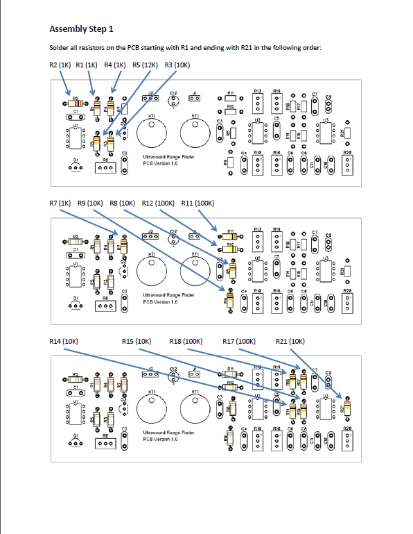
1. Print the top component silkscreen and board outline artwork on a plain piece of paper and measure the board outline to make sure the dimensions are accurate. Some printers do not print to scale and you may have to change the print scale in your PCB application to get the correct size on paper.
2. Cut out a piece of 1/4" foam board the same size as the board outline.
3. Tape the properly scaled top component silkscreen artwork to the foam board.
4. Using the tip of a sharp pencil or a small push drill, make small holes through the foam board where the component leads go.
5. Test fit each component to make sure all the parts will fit on the PCB as marked. Make any outline adjustments in the PCB software until all parts fit.
6. If everything fits, take one sheet of paper from the printer and write "Side A" on one side and "Side B" on the other. Load the marked sheet of paper into the printer with the "Side A" mark facing up and then print the bottom trace artwork.
7. Observe which side of the paper the trace artwork was printed on (Side A or Side B). If the trace artwork printed on Side A, remember to load the printer with PCBFX toner transfer paper glossy side up. If the trace artwork printed on Side B, remember to load the printer with PCBFX toner transfer paper glossy side down.
Note: I usually load the printer with two sheets of PCBFX toner transfer paper. I print multiple copies of the trace side artwork on one sheet, and multiple copies of the component side silkscreen on the other sheet. That way if I make a mistake applying the artwork to the PCB, I can always cut out another copy and try again.
8. Turn on the laminator and set the temperature according to the PCBFX instruction sheet.
9. Fill a sink or other container large enough to hold the PCB with cold water.
10. Cut the blank PCB so that it is at least 1/8" larger than the board outline. Many times the PCB edges will be raised slightly after cutting which can interfere with toner transfer. The extra space helps ensure that heat and pressure are evenly applied to traces at the edge of the board.
11. Carefully clean the blank PCB copper surfaces to remove any slight tarnish or oil. The cleaning process should leave a slight haze on the copper that will help the toner to grip the board. Deep scratches or excessive hazing are bad so don't go overboard on the cleaning process. I clean the PCB first with liquid dish washing detergent and a polishing cloth, and then follow up with alcohol and a lint free cloth.
12. Load the PCBFX toner transfer paper into the printer using care to only touch the corners or edges where artwork will not be printed.
13. Print the artwork with the toner density setting as high as possible to achieve a dark opaque print. Be sure to use the "mirror image" setting on your PCB software so that when the transfer paper is applied the traces and text are applied correctly.
14. Trim the artwork closely to the board outline on the long edges but leave at least one to two inches on one of the short edges. Use care not to touch the applied toner with tools or fingers while trimming.
15. Place the artwork face down and centered on the clean and dry copper side of the PCB. Fold over the extra length of paper and carefully insert the PCB into the laminator folded edge first.
Note: I repeat the lamination step a few times to make sure the toner has completely fused to the copper. You may not need to do that with the newer laminators supported by Pulsar Professional FX.
16. Immediately after laminating the board, submerge it under cold water. The paper will almost immediately darken and begin to separate from the fused artwork. Wait at least 30 seconds and gently slide the paper away from the board.
17. Carefully rinse the board and pat dry with a soft cloth. Let the board fully dry before proceeding to the next step.
Note: PCBFX recommends a second lamination step to seal the toner and fill in any tiny voids that might leave holes during etching. I've tried the process with and without the sealing step and saw distinct improvement in the quality of the PCB when the sealing step is used. Especially with large dark areas prone to tiny pinhole voids and very thin traces.
18. Cut a piece of the green sealing strip to the same size as the PCB but leaving one to two inches on one of the short sides to be folded over during laminating.
19. Place the green sealing strip over the toner, fold the excess over, and feed the PCB into the laminator using slight finger pressure on the sealing strip to keep it feeding straight.
Note: I usually run the board through the laminator a few times to make sure the sealer is completely applied. You may not need to do that with the newer laminators supported by Pulsar Professional FX.
20. Peal the sealing strip from the PCB. The board is now ready for etching.
I've found that it's not necessary to use a whole tank of chemicals to etch a board. I set my PCB software to fill in empty areas of the PCB with copper which reduces the amount of chemical required and the amount of time needed, both of which help improve the quality of the etching. I use two containers: One large enough for the board, and the other large enough to hold the first container and an inch or so of hot water. I heat up some water to near boiling and pour it in the large container. Then I pour just enough chemical into the small container to cover the board, set it in the large container, and let the chemical warm up. After that I use a disposable sponge brush to gently brush the chemical onto the board until etching is complete. I can etch a board in about 5 minutes using about two ounces of Ferric Chloride.
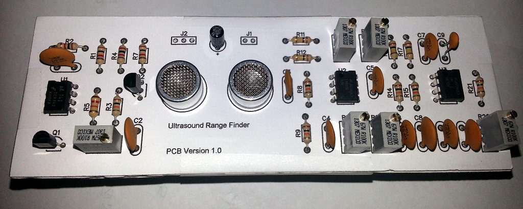
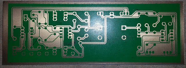
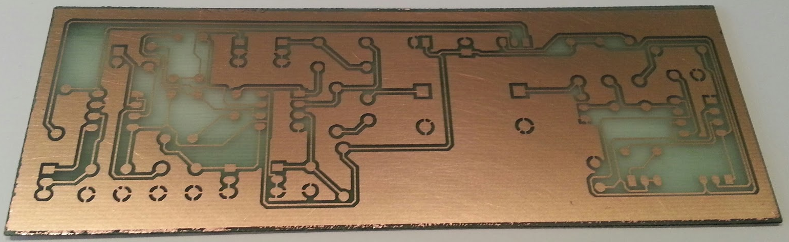
Below are some photos of the board after etching and after the component silkscreen layer artwork was applied and holes drilled. It only took me about 45 minutes to do everything I wanted to do including drill the holes. And I really liked the way the board looked when I was done so the effort was worthwhile. The boards made with PCBFX are the best I've done outside of a professional fabrication studio and I'm using it for all of my DIY projects.
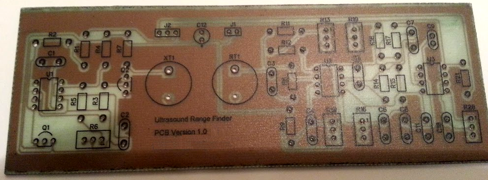
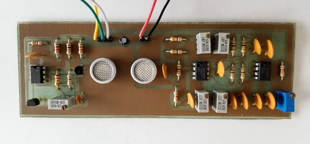
The completed Analog Ultrasound Range Finder is shown below.
Please Note: I have no business relationship with PCBFX. Nothing of financial value was exchanged for my recommendation. PCBFX provided no compensation of any kind during the creation of this project. I will not be compensated in any way if you choose to build this project or purchase supplies from PCBFX. I simply had a good experience with PCBFX and believe you will too.
Follow the Steps in the Assembly Manual to Build and Test the Range Finder
The assembly manual contains four sections of interest to the builder:
1. Basic assembly hints - Useful hints for the new builder.
2. Detailed assembly instructions - Shows what parts go where at each step in the process.
3. Test and Alignment procedure - Verifying the assembly and getting it ready for work.
4. Troubleshooting procedure - Just in case something goes wrong.
After the PCB has been fabricated, follow the steps in the assembly manual to build the Ultrasound Range Finder. The troubleshooting section will help you find and fix anything isn't working correctly.
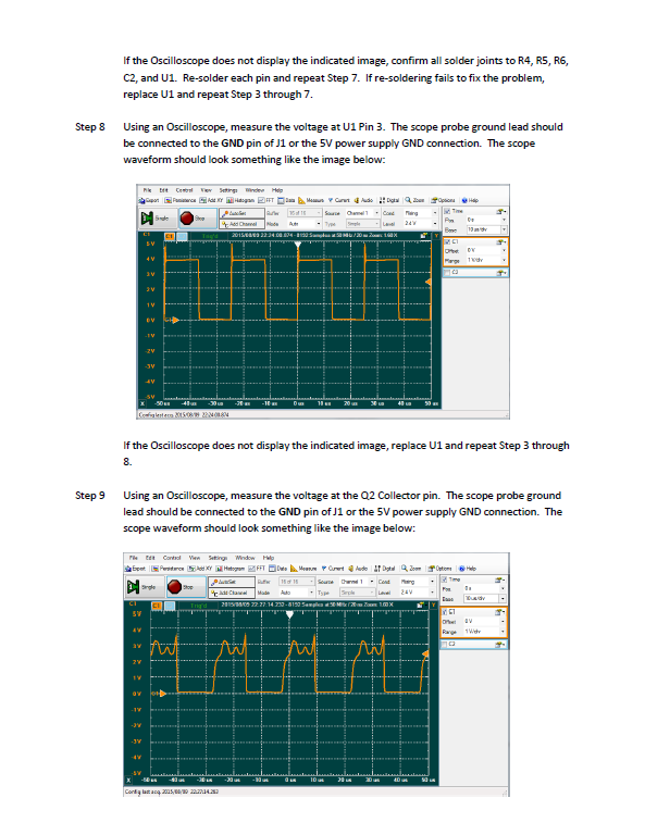
After the range finder has been assembled and tested, an oscilloscope can be attached to the Transmitter Enable (TE) and Carrier Detect (CD) output to view the receiver and transmitter in action. The oscilloscope trace below shows the TE pin in red enabling the 40KHz oscillator. The blue trace shows the output of the PLL detector. Notice that because the receiver is so close to the transmitter when TE is enabled that the CD output goes low while transmitting and then inactive after transmission stops. A short time later, the CD pin goes low again indicating a reflection has been detected. A microprocessor will be used to measure the time delay and convert it to a distance.
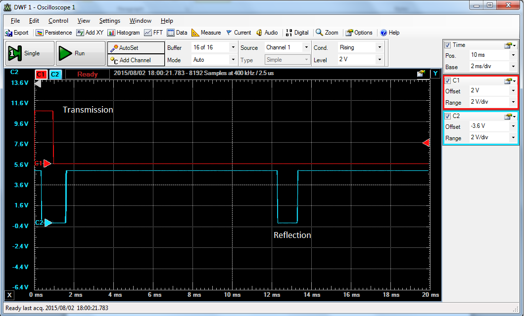
The second scope trace shows the raw limiter output to the Carrier Detector in green with the CD signal in blue. The Carrier Detector does indeed change state after receiving at least 20 cycles of 40KHz carrier.
Attach the Range Finder to the Micro-controller of Your Choice
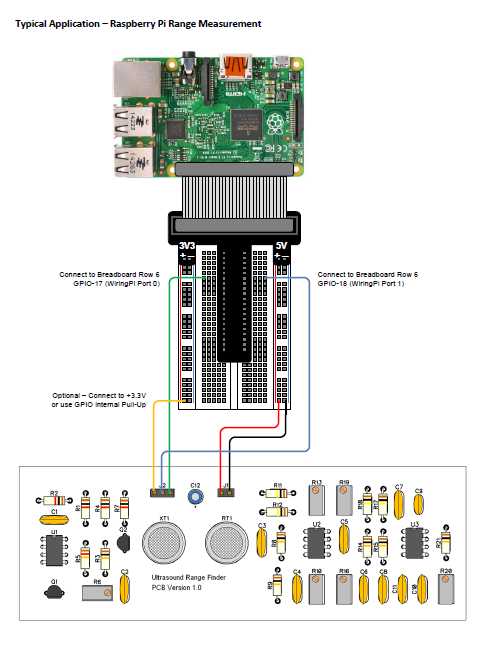
A datasheet for the Analog Ultrasound Range Finder can be found HERE.
The datasheet is a quick reference for the operating parameters of the range finder board and contains some examples for interfacing to the Raspberry Pi and TI MSP430. I did not have an Arduino board on hand to test with prior to writing this article so I won't cover it here to avoid misleading folks that want to use it. Those familiar with the Arduino family of micro controllers will readily understand how to use the simple range finder interface.
Compile and Run the Example Software
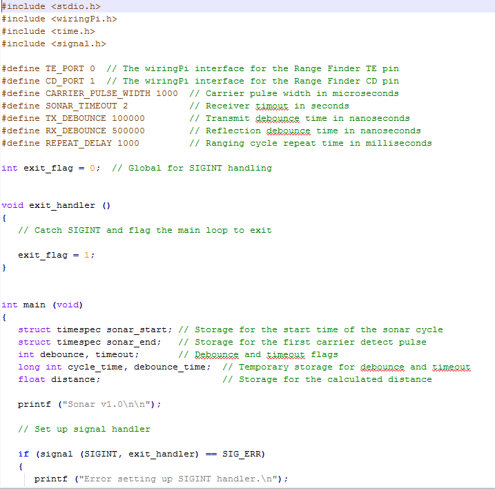
I've created a sample C program for exercising the functionality of the Ultrasound Range Finder which can be downloaded HERE.
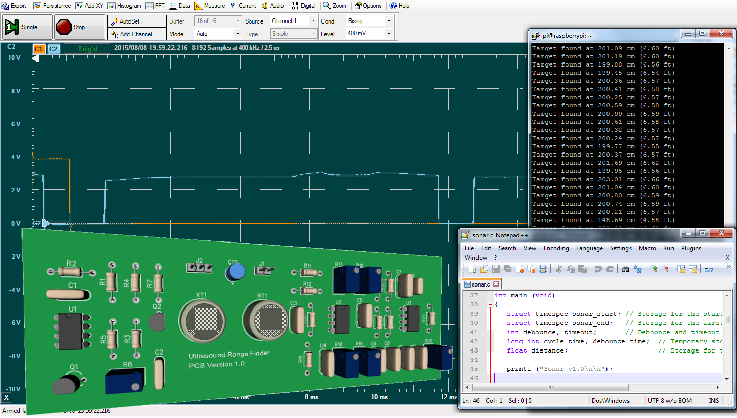
The sonar application works in similar fashion to the IP PING utility. It generates a 1ms pulse of 40KHz ultrasound and then waits to receive an ultrasound reflection. If a target reflection is found, the target distance is automatically calculated and displayed in cm and feet. Targets are "pinged" every second until the user presses Ctrl-C.
The sonar application was compiled and tested on the Raspberry Pi 2 running Raspbian 1.4.1 and makes use of the excellent WiringPi library from Gordon Henderson which can be found at his website. The WiringPi library contains function calls similar to those found on the Arduino so it is possible to rearrange the example program to run on the Arduino platform.
The steps below describe how to build the sonar application:
1. If the WiringPi library is not already installed on your Raspberry Pi, follow the library install instructions here.
2. Download the sonar.c source file and copy it to a directory on the Raspberry Pi.
3. Build the sonar executable by entering the following command:
gcc sonar.c -o sonar -lwiringPi
4. Execute the sonar application by entering the following command:
sudo ./sonar
The sonar application will display a "Target Found..." message every second or a "Timeout" message every 2 seconds depending on whether or not an ultrasound reflection was detected.
It's possible to add multi-target detection, a UI with a bar graph showing where targets ahead are located, a display with target distance changes over time, and much more. I've left these to the reader to implement.